Introduction
UART (Universal Asynchronous Receiver/Transmitter) is a serial communication protocol in which data is transferred serially bit by bit at a time. Asynchronous serial communication is widely used for byte oriented transmission. In Asynchronous serial communication, a byte of data is transferred at a time.
UART serial communication protocol uses a defined frame structure for their data bytes.Frame structure in Asynchronous communication consists :
- START bit: It is a bit with which indicates that serial communication has started and it is always low.
- Data bits packet: Data bits can be packets of 5 to 9 bits. Normally we use 8 bit data packet, which is always sent after the START bit.
STOP bit: This usually is one or two bits in length. It is sent after data bits packet to indicate the end of frame. Stop bit is always logic high.
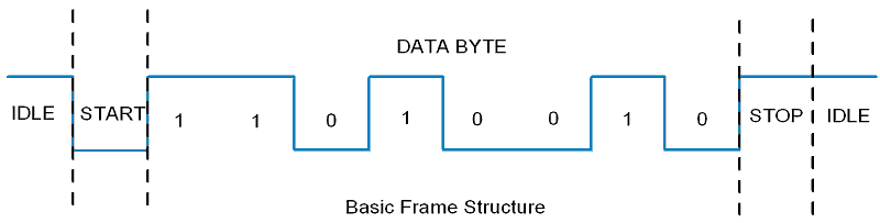
Usually, an asynchronous serial communication frame consists of a START bit (1 bit) followed by a data byte (8 bits) and then a STOP bit (1 bit), which forms a 10-bit frame as shown in the figure above. The frame can also consist of 2 STOP bits instead of a single bit, and there can also be a PARITY bit after the STOP bit.
LPC2148 UART
LPC2148 has two inbuilt UARTs available i.e. UART0&UART1. So, we can connect two UART enabled devices (GSM module, GPS module, Bluetooth module etc.) with LPC2148 at a time.
UART0 and UART1 are identical other than the fact that UART1 has modem interface included.
Features of UART0
- 16 byte Receive and Transmit FIFOs
- Built-in fractional baud rate generator with autobauding capabilities
- Software flow control through TXEN bit in Transmit Enable Register
Features of UART1
- 16 byte Receive and Transmit FIFOs
- Built-in fractional baud rate generator with autobauding capabilities
- Software and hardware flow control implementation possible
- Standard modem interface signals included with flow control (auto-CTS/RTS) fully supported in hardware
LPC2148 UART Pins
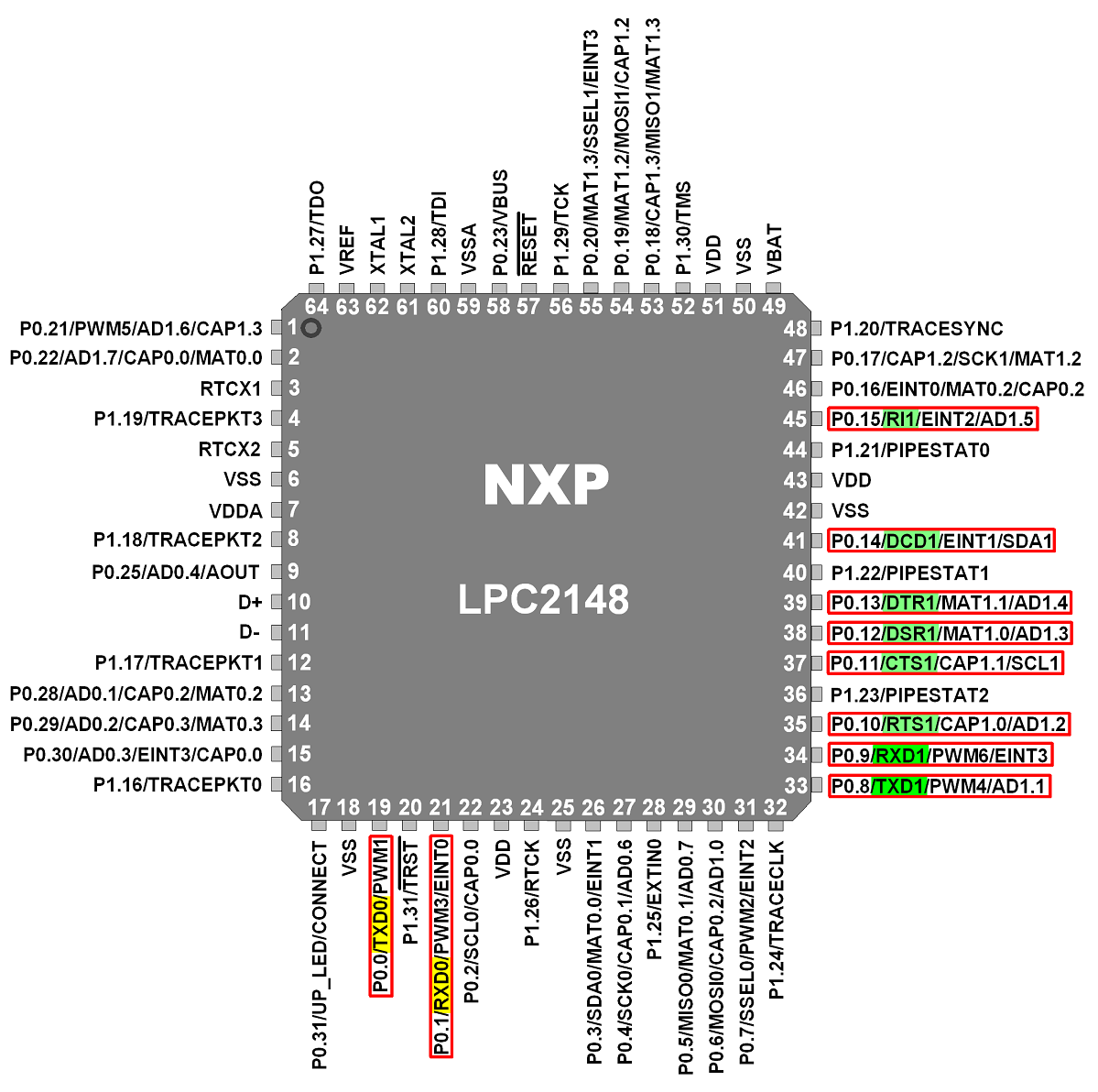
UART0 :
TXD0 (Output pin): Serial Transmit data pin.
RXD0 (Input pin): Serial Receive data pin.
UART1 :
TXD1 (Output pin): Serial Transmit data pin.
RXD1 (Input pin): Serial Receive data pin.
RTS1 (Output pin): Request To Send signal pin. Active low signal indicates that the UART1 would like to transmit data to the external modem.
CTS1 (Input pin): Clear To Send signal pin. Active low signal indicates if the external modem is ready to accept transmitted data via TXD1 from the UART1.
DSR1 (Input pin): Data Set Ready signal pin. Active low signal indicates if the external modem is ready to establish a communication link with the UART1.
DTR1 (Output pin): Data Terminal Ready signal pin. Active low signal indicates that the UART1 is ready to establish connection with external modem.
DCD1 (Input pin): Data Carrier Detect signal pin. Active low signal indicates if the external modem has established a communication link with the UART1 and data may be exchanged.
RI1 (Input pin): Ring Indicator signal pin. Active low signal indicates that a telephone ringing signal has been detected by the modem.
We will be seeing how to use UART0 here. UART1 can be used in a similar way by using the corresponding registers for UART1.
UART0 Registers
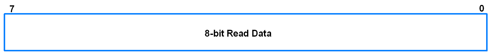
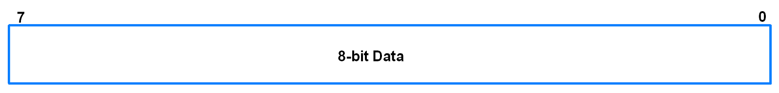
1. U0RBR (UART0 Receive Buffer Register)
- It is an 8-bit read only register.
- This register contains the received data.
- It contains the “oldest” received byte in the receive FIFO.
- If the character received is less than 8 bits, the unused MSBs are padded with zeroes.
- The Divisor Latch Access Bit (DLAB) in U0LCR must be zero in order to access the U0RBR. (DLAB = 0)
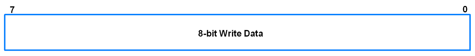
2. U0THR (UART0 Transmit Holding Register)
- It is an 8-bit write only register.
- Data to be transmitted is written to this register.
- It contains the “newest” received byte in the transmit FIFO.
- The Divisor Latch Access Bit (DLAB) in U0LCR must be zero in order to access theU0THR. (DLAB = 0)
3. U0DLL and U0DLM (UART0 Divisor Latch Registers)
- U0DLL is the Divisor Latch LSB.
- U0DLM is the Divisor Latch MSB.
- These are 8-bit read-write registers.
- UART0 Divisor Latch holds the value by which the PCLK(Peripheral Clock) will be divided. This value must be 1/16 times the desired baud rate.
- A 0x0000 value is treated like a 0x0001 value as division by zero is not allowed.
- The Divisor Latch Access Bit (DLAB) in U0LCR must be one in order to access the UART0 Divisor Latches. (DLAB = 1)

4. U0FDR (UART0 Fractional Divider Register)
- It is a 32-bit read write register.
- It decides the clock pre-scalar for baud rate generation.
- If fractional divider is active (i.e. DIVADDVAL>0) and DLM = 0, DLL must be greater than 3.
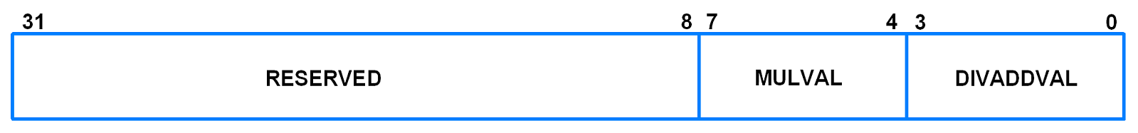
- If DIVADDVAL is 0, the fractional baudrate generator will not impact the UART0 baudrate.
- Reset value of DIVADDVAL is 0.
- MULVAL must be greater than or equal to 1 for UART0 to operate properly, regardless of whether the fractional baudrate generator is used or not.
- Reset value of MULVAL is 1.
- The formula for UART0 baudrate is given below
- MULVAL and DIVADDVAL should have values in the range of 0 to 15. If this is not ensured, the output of the fractional divider is undefined.
- The value of the U0FDR should not be modified while transmitting/receiving data. This may result in corruption of data.
5. U0IER (UART0 Interrupt Enable Register)
- It is a 32-bit read-write register.
- It is used to enable UART0 interrupt sources.
- DLAB should be zero (DLAB = 0).
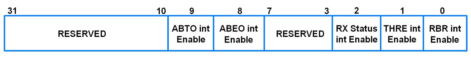
- Bit 0 - RBR Interrupt Enable. It also controls the Character Receive Time-Out interrupt.
0 = Disable Receive Data Available interrupt
1 = Enable Receive Data Available interrupt - Bit 1 - THRE Interrupt Enable
0 = Disable THRE interrupt
1 = Enable THRE interrupt - Bit 2 - RX Line Interrupt Enable
0 = Disable UART0 RX line status interrupts
1 = EnableUART0 RX line status interrupts - Bit 8 - ABEO Interrupt Enable
0 = Disable auto-baud time-out interrupt
1 = Enable auto-baud time-out interrupt - Bit 9 - ABTO Interrupt Enable
0 = Disable end of auto-baud interrupt
1 = Enable the end of auto-baud interrupt
6. U0IIR (UART0 Interrupt Identification Register)
- It is a 32-bit read only register.
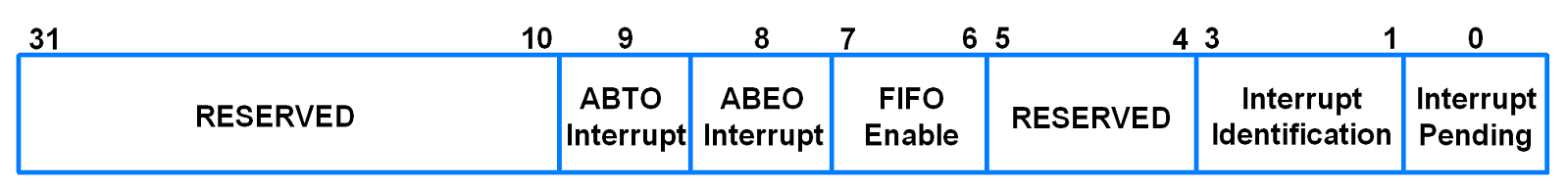
- It provides a status code that denotes the priority and source of a pending interrupt.
- It must be read before exiting the Interrupt Service Routine to clear the interrupt.
- Bit 0 - Interrupt Pending
0 = At least one interrupt is pending
1 = No interrupts pending - Bit 3:1 - Interrupt Identification
Identifies an interrupt corresponding to theUART0 Rx FIFO.
011 = Receive Line Status (RLS) Interrupt
010 = Receive Data Available (RDA) Interrupt
110 = Character Time-out Indicator (CTI) Interrupt
001 = THRE Interrupt - Bit 7:6 - FIFO EnableThese bits are equivalent to FIFO enable bit in FIFO Control Register,
0 = If FIFOs are disabled
1 = FIFOs are enabled - Bit 8 - ABEO Interrupt
If interrupt is enabled,
0 = No ABEO interrupt
1 = Auto-baud has finished successfully - Bit 9 - ABTO Interrupt
If interrupt is enabled,
0 = No ABTO interrupt
1 = Auto-baud has timed out
7. U0LCR (UART0 Line Control Register)
- It is an 8-bit read-write register.
- It determines the format of the data character that is to be transmitted or received.
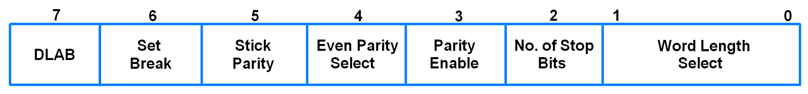
- Bit 1:0 - Word Length Select
00 = 5-bit character length
01 = 6-bit character length
10 = 7-bit character length
11 = 8-bit character length - Bit 2 - Number of Stop Bits
0 = 1 stop bit
1 = 2 stop bits - Bit 3 - Parity Enable
0 = Disable parity generation and checking
1 = Enable parity generation and checking - Bit 5:4 - Parity Select
00 = Odd Parity
01 = Even Parity
10 = Forced “1” Stick Parity
11 = Forced “0” Stick Parity - Bit 6 - Break Control
0= Disable break transmission
1 = Enable break transmission - Bit 7 - Divisor Latch Access Bit (DLAB)
0 = Disable access to Divisor Latches
1 = Enable access to Divisor Latches
8. U0LSR (UART0 Line Status Register)
- It is an 8-bit read only register.
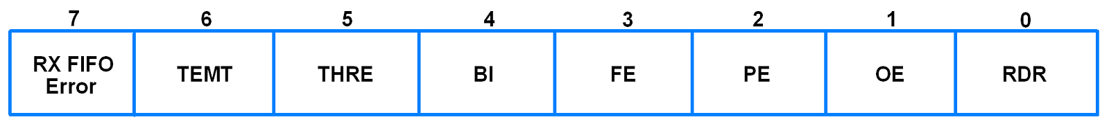
- It provides status information on UART0 RX and TX blocks.
- Bit 0 - Receiver Data Ready
0 = U0RBR is empty
1 = U0RBR contains valid data - Bit 1 - Overrun Error
0 = Overrun error status inactive
1 = Overrun error status active
This bit is cleared when U0LSR is read. - Bit 2 - Parity Error
0 = Parity error status inactive
1 = Parity error status active
This bit is cleared when U0LSR is read. - Bit 3 - Framing Error
0 = Framing error status inactive
1 = Framing error status active
This bit is cleared when U0LSR is read. - Bit 4 - Break Interrupt
0 = Break interrupt status inactive
1 = Break interrupt status active
This bit is cleared when U0LSR is read. - Bit 5 - Transmitter Holding Register Empty
0 = U0THR has valid data
1 = U0THR empty - Bit 6 - Transmitter Empty
0 = U0THR and/or U0TSR contains valid data
1 = U0THR and U0TSR empty - Bit 7 - Error in RX FIFO (RXFE)
0 = U0RBR contains no UART0 RX errors
1 = U0RBR contains at least one UART0 RX error
This bit is cleared when U0LSR is read.
9. U0TER (UART0 Transmit Enable Register)
- It is an 8-bit read-write register.
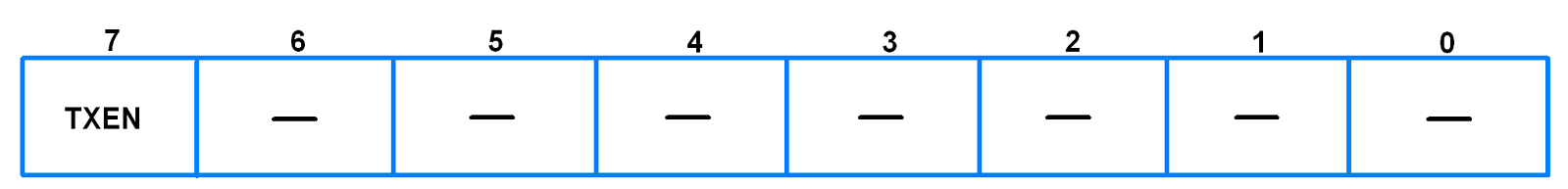
- The U0TER enables implementation of software flow control. When TXEn=1, UART0 transmitter will keep sending data as long as they are available. As soon as TXEn becomes 0, UART0 transmission will stop.
- Software implementing software-handshaking can clear this bit when it receives an XOFF character (DC3). Software can set this bit again when it receives an XON (DC1) character.
- Bit 7 : TXEN
0 = Transmission disabled
1 = Transmission enabled - If this bit is cleared to 0 while a character is being sent, the transmission of that character is completed, but no further characters are sent until this bit is set again.
Programming of UART0
1. Initialization of UART0
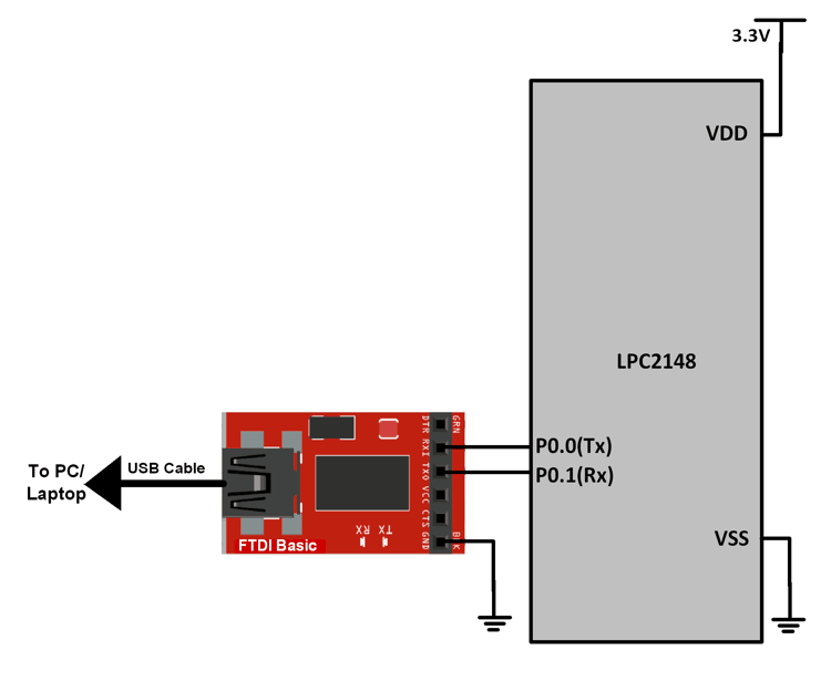
- Configure P0.0 and P0.1 as TXD0 and RXD0 by writing 01 to the corresponding bits in PINSEL0.
- Using U0LCR register, make DLAB = 1. Also, select 8-bit character length and 1 stop bit.
- Set appropriate values in U0DLL and U0DLM depending on the PCLK value and the baud rate desired. Fractional divider can also be used to get different values of baudrate.
- Example,
PCLK = 15MHz. For baud rate 9600, without using fractional divider register, from the baud rate formula, we have,
On reset, MulVal = 1 and DivAddVal = 0 in the Fractional Divider Register.
Hence,
( 256 x U0DLM + U0DLL ) = 97.65
We can consider it to be 98 or 97. It will make the baud rate slightly less or more than 9600. This small change is tolerable. We will consider 97.
Since 97 is less than 256 and register values cannot contain fractions, we will take U0DLM = 0. This will give U0DLM = 97. - Make DLA = 0 using U0LCR register.
void UART0_init(void)
{
	PINSEL0 = PINSEL0 | 0x00000005;	/* Enable UART0 Rx0 and Tx0 pins of UART0 */
	U0LCR = 0x83;	 /* DLAB = 1, 1 stop bit, 8-bit character length */
	U0DLM = 0x00;	/* For baud rate of 9600 with Pclk = 15MHz */
	U0DLL = 0x61;		/* We get these values of U0DLL and U0DLM from formula */
	U0LCR = 0x03; 	/* DLAB = 0 */
}
2. Receiving character
- Monitor the RDR bit in U0LSR register to see if valid data is available in U0RBR register.
unsigned char UART0_RxChar(void) /*A function to receive a byte on UART0 */
{
	while( (U0LSR & 0x01) == 0);	/*Wait till RDR bit becomes 1 which tells that receiver contains valid data */
		return U0RBR;
}
3. Transmitting character
- Monitor the THRE bit in U0LSR register. When this bit becomes 1, it indicates that U0THR register is empty and the transmission is completed.
void UART0_TxChar(char ch) /*A function to send a byte on UART0 */
{
	U0THR = ch;
	while( (U0LSR & 0x40) == 0 );	/* Wait till THRE bit becomes 1 which tells that transmission is completed */
}
Example
Program for echo test. LPC 2148 will receive a character through PC terminal and will transmit the same character back to the PC terminal.
Software like RealTerm, Putty can be used for this on PC.
Program
/*
  UART0 in LPC2148(ARM7)
  http://www.electronicwings.com/arm7/lpc2148-uart0
*/

#include <lpc214x.h>
#include <stdint.h>
#include "UART.h"

int main(void)
{
	char receive;
	UART0_init();
	while(1)
	{
		receive = UART0_RxChar();
		UART0_SendString("Received:");
		UART0_TxChar(receive);
		UART0_SendString("\r\n");
	}
}
Video
Using Interrupt
In the above example, we have used the polling method to wait for setting of bits on completion of transmission or reception. We can use interrupts instead. Interrupts allow the controller to process other data while waiting on a certain task.
To use interrupts, we need to use the interrupt registers of UART0 and the VIC (Vectored Interrupt Controller) registers. The connections will be same as shown for above example.
Program using Interrupt
/*
  UART0 in LPC2148(ARM7) using Interrupt
  http://www.electronicwings.com/arm7/lpc2148-uart0
*/

#include <lpc214x.h>
#include <stdint.h>

char rx;

__irq void UART0_Interrupt(void);

void UART0_init(void)
{
	PINSEL0 = PINSEL0 | 0x00000005;	/* Enable UART0 Rx0 and Tx0 pins of UART0 */
	U0LCR = 0x83;	/* DLAB = 1, 1 stop bit, 8-bit character length */
	U0DLM = 0x00;	/* For baud rate of 9600 with Pclk = 15MHz */
	U0DLL = 0x61;	/* We get these values of U0DLL and U0DLM from formula */
	U0LCR = 0x03; /* DLAB = 0 */
	U0IER = 0x00000003;	/* Enable THRE and RBR interrupt */
}


__irq void UART0_Interrupt(void)
{
	int iir_value;
	iir_value = U0IIR;
	while ( !(iir_value & 0x01) );
	if( iir_value & 0x00000004 )
	{
		rx = U0RBR;
	}
		U0THR = rx;
		while( (U0LSR & 0x40) == 0 );
	VICVectAddr = 0x00;
}


int main(void)
{
	UART0_init();
	VICVectAddr0 = (unsigned) UART0_Interrupt;	/* UART0 ISR Address */
	VICVectCntl0 = 0x00000026;	/* Enable UART0 IRQ slot */
	VICIntEnable = 0x00000040;	/* Enable UART0 interrupt */
	VICIntSelect = 0x00000000;	/* UART0 configured as IRQ */
	while(1);
}
Video
Components Used |
||
|---|---|---|
| ARM7 LPC2148 ARM7 LPC2148 |
X 1 | |
| CP2103 USB TO UART BRIDGE CP2103 is single chip USB to UART Bridge. It supports USB 2.0 protocol. |
X 1 | |