Introduction to ADC
Analog to Digital Converter(ADC) is used to convert analog signal into digital form. LPC2148 has two inbuilt 10-bit ADC i.e. ADC0 & ADC1.
- ADC0 has 6 channels &ADC1 has 8 channels.
- Hence, we can connect 6 distinct types of input analog signals to ADC0 and 8 distinct types of input analog signals to ADC1.
- ADCs in LPC2148 use Successive Approximation technique to convert analog signal into digital form.
- This Successive Approximation process requires a clock less than or equal to 4.5 MHz. We can adjust this clock using clock divider settings.
- Both ADCs in LCP2148 convert analog signals in the range of 0V to VREF (typically 3V; not to exceed VDDA voltage level).
ARM LPC4128 ADC Pins
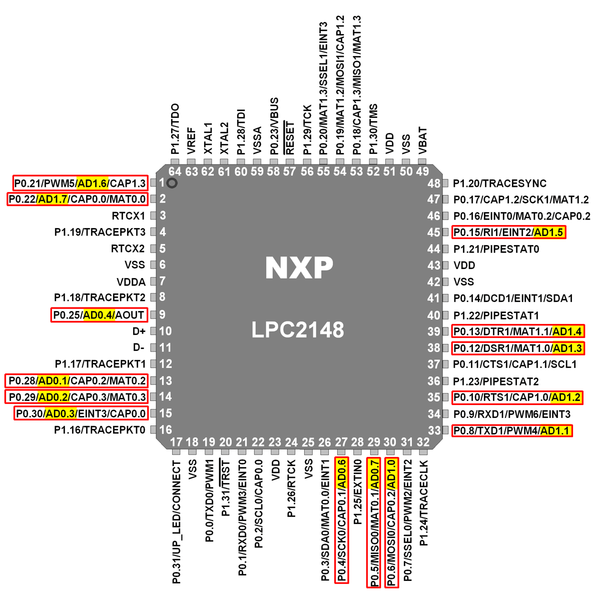
AD0.1:4, AD0.6:7 & AD1.7:0 (Analog Inputs)
These are Analog input pins of ADC. If ADC is used, signal level on analog pins must not be above the level of VDDA; otherwise, ADC readings will be invalid. If ADC is not used, then the pins can be used as 5V tolerant digital I/O pins.
VREF (Voltage Reference)
Provide Voltage Reference for ADC.
VDDA& VSSA (Analog Power and Ground)
These are the power and ground pins for ADC. These should be same as VDD & VSS.
Let’s see the ADC registers which are used to control and monitors the ADC operation.
Here, we will see ADC0 registers and their configurations. ADC1 has similar registers and can be configured in a similar manner.
ADC0 Registers Configuration
1. AD0CR (ADC0 Control Register)
- AD0CR is a 32-bit register.
- This register must be written to select the operating mode before A/D conversion can occur.
- It is used for selecting channel of ADC, clock frequency for ADC, number of clocks or number of bits in result, start of conversion and few other parameters.
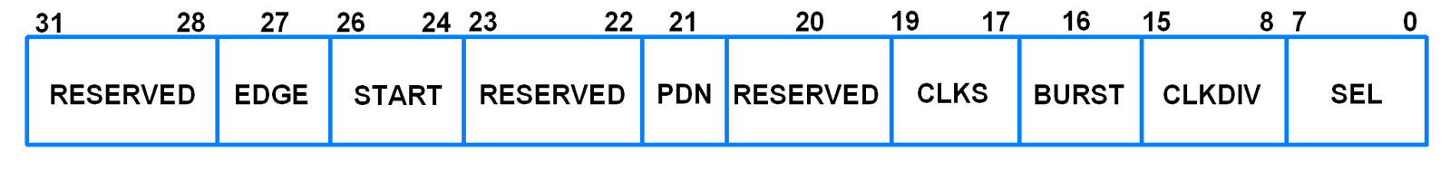
- Bits 7:0 – SEL
These bits select ADC0 channel as analog input. In software-controlled mode, only one of these bits should be 1.e.g. bit 7 (10000000) selects AD0.7 channel as analog input. - Bits 15:8 – CLKDIV
The APB(ARM Peripheral Bus)clock is divided by this value plus one, to produce the clock for ADC.
This clock should be less than or equal to 4.5MHz. - Bit 16 – BURST
0 = Conversions are software controlled and require 11 clocks
1 = In Burst mode ADC does repeated conversions at the rate selected by the CLKS field for the analog inputs selected by SEL field. It can be terminated by clearing this bit, but the conversion that is in progress will be completed.
When Burst = 1, the START bits must be 000, otherwise the conversions will not start. - Bits 19:17 – CLKS
Selects the number of clocks used for each conversion in burst mode and the number of bits of accuracy of Result bits of AD0DR.
e.g. 000 uses 11 clocks for each conversion and provide 10 bits of result in corresponding ADDR register.
000 = 11 clocks / 10 bits
001 = 10 clocks / 9 bits
010 = 9 clocks / 8 bits
011 = 8 clocks / 7 bits
100 = 7 clocks / 6 bits
101 = 6 clocks / 5 bits
110 = 5 clocks / 4 bits
111 = 4 clocks / 3 bits - Bit 20 – RESERVED
- Bit 21 – PDN
0 = ADC is in Power Down mode
1 = ADC is operational - Bit 23:22 – RESERVED
- Bit 26:24 – START
When BURST bit is 0, these bits control whether and when A/D conversion is started
000 = No start (Should be used when clearing PDN to 0)
001 = Start conversion now
010 = Start conversion when edge selected by bit 27 of this register occurs on CAP0.2/MAT0.2 pin
011= Start conversion when edge selected by bit 27 of this register occurs on CAP0.0/MAT0.0 pin
100 = Start conversion when edge selected by bit 27 of this register occurs on MAT0.1 pin
101 = Start conversion when edge selected by bit 27 of this register occurs on MAT0.3 pin
110 = Start conversion when edge selected by bit 27 of this register occurs on MAT1.0 pin
111 = Start conversion when edge selected by bit 27 of this register occurs on MAT1.1 pin - Bit 27 – EDGE
This bit is significant only when the Start field contains 010-111. In these cases,
0 = Start conversion on a rising edge on the selected CAP/MAT signal
1 = Start conversion on a falling edge on the selected CAP/MAT signal - Bit 31:28 – RESERVED
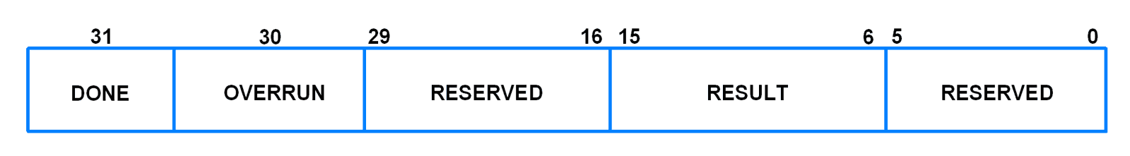
2. AD0GDR (ADC0 Global Data Register)
- AD0GDR is a 32-bit register.
- This register contains the ADC’s DONE bit and the result of the most recent A/D conversion.
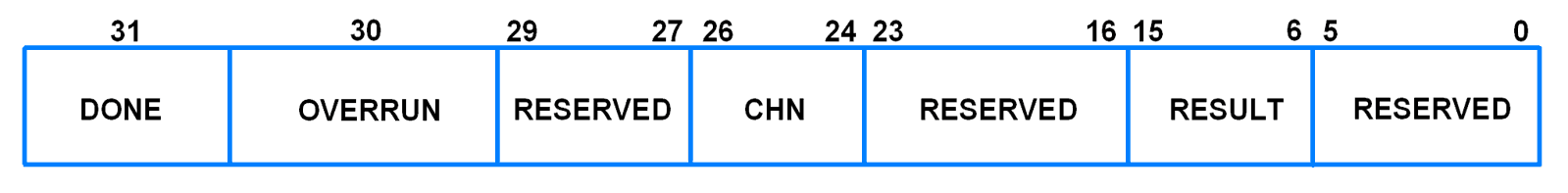
- Bit 5:0 – RESERVED
- Bits 15:6 – RESULT
When DONE bit is set to 1, this field contains 10-bit ADC result that has a value in the range of 0 (less than or equal to VSSA) to 1023 (greater than or equal to VREF). - Bit 23:16 – RESERVED
- Bits 26:24 – CHN
These bits contain the channel from which ADC value is read.
e.g. 000 identifies that the RESULT field contains ADC value of channel 0. - Bit 29:27 – RESERVED
- Bit 30 – Overrun
This bit is set to 1 in burst mode if the result of one or more conversions is lost and overwritten before the conversion that produced the result in the RESULT bits.
This bit is cleared by reading this register. - Bit 31 – DONE
This bit is set to 1 when an A/D conversion completes. It is cleared when this register is read and when the AD0CR is written.
If AD0CR is written while a conversion is still in progress, this bit is set and new conversion is started.
3. ADGSR (A/D Global Start Register)
- ADGSR is a 32-bit register.
- Software can write to this register to simultaneously start conversions on both ADC.

- BURST (Bit 16), START (Bit <26:24>) & EDGE (Bit 27)
These bits have same function as in the individual ADC control registers i.e. AD0CR & AD1CR. Only difference is that we can use these function for both ADC commonly from this register.
4. AD0STAT (ADC0 Status Register)
- AD0STAT is a 32-bit register.
- It allows checking of status of all the A/D channels simultaneously.
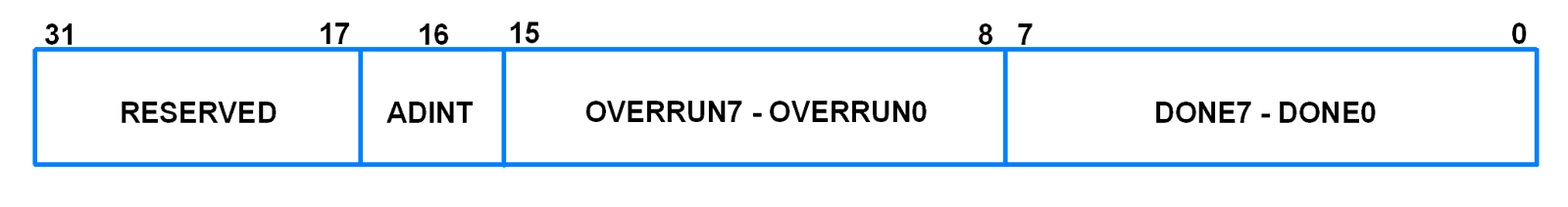
- Bit 7:0 – DONE7:DONE0
These bits reflect the DONE status flag from the result registers for A/D channel 7 - channel 0. - Bit 15:8 – OVERRUN7:OVERRUN0
These bits reflect the OVERRUN status flag from the result registers for A/D channel 7 - channel 0. - Bit 16 – ADINT
This bit is 1 when any of the individual A/D channel DONE flags is asserted and enables ADC interrupt if any of interrupt is enabled in AD0INTEN register. - Bit 31:17 – RESERVED
5. AD0INTEN (ADC0 Interrupt Enable)
- AD0INTEN is a 32-bit register.
- It allows control over which channels generate an interrupt when conversion is completed.
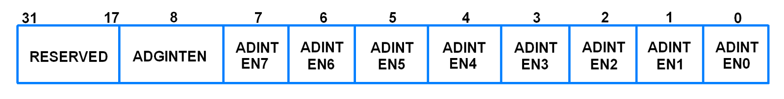
- Bit 0 – ADINTEN0
0 = Completion of a A/D conversion on ADC channel 0 will not generate an interrupt
1 = Completion of a conversion on ADC channel 0 will generate an interrupt - Remaining ADINTEN bits have similar description as given for ADINTEN0.
- Bit 8 – ADGINTEN
0 = Only the individual ADC channels enabled by ADINTEN7:0 will generate interrupts
1 = Only the global DONE flag in A/D Data Register is enabled to generate an interrupt
6. AD0DR0-AD0DR7 (ADC0 Data Registers)
- These are 32-bit registers.
- They hold the result when A/D conversion is completed.
- They also include flags that indicate when a conversion has been completed and when a conversion overrun has occurred.
- Bit 5:0 – RESERVED
- Bits 15:6 – RESULT
When DONE bit is set to 1, this field contains 10-bit ADC result that has a value in the range of 0 (less than or equal to VSSA) to 1023 (greater than or equal to VREF). - Bit 29:16 – RESERVED
- Bit 30 – Overrun
This bit is set to 1 in burst mode if the result of one or more conversions is lost and overwritten before the conversion that produced the result in the RESULT bits.
This bit is cleared by reading this register. - Bit 31 – DONE
This bit is set to 1 when an A/D conversion completes. It is cleared when this register is read.
Steps for Analog to Digital Conversion
- Configure the ADxCR (ADC Control Register) according to the need of application.
- Start ADC conversion by writing appropriate value to START bits in ADxCR. (Example, writing 001 to START bits of the register 26:24, conversion is started immediately).
- Monitor the DONE bit (bit number 31) of the corresponding ADxDRy (ADC Data Register) till it changes from 0 to 1. This signals completion of conversion. We can also monitor DONE bit of ADGSR or the DONE bit corresponding to the ADC channel in the ADCxSTAT register.
- Read the ADC result from the corresponding ADC Data Register.
ADxDRy. E.g. AD0DR1 contains ADC result of channel 1 of ADC0.
Read Analog Voltage using LPC2148
Let’s write a program to convert input voltage signal on AD0.1 (P0.28) into digital signal. We will convert the digital value to equivalent voltage value and display it on an LCD. We can compare this voltage with actual voltage measured on a digital multimeter.
Interfacing Diagram
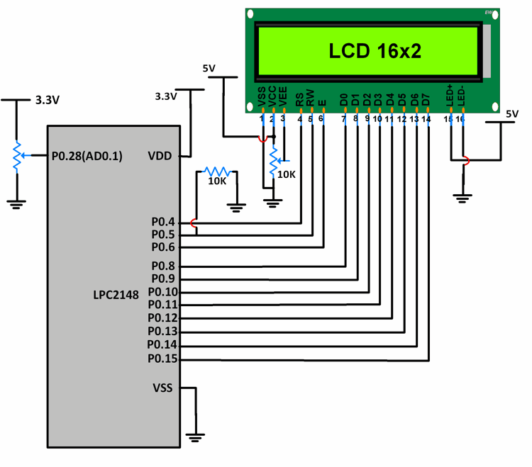
Here, input signal is a DC signal which varies from 0 to 3.3V via a potentiometer.
Signal is given on P0.28. P0.28 is configured as AD0.1 using PINSEL register.
10-bit ADC result is stored in a variable and its lower 8 bits are given to P0.8-P0.15. These pins are connected to the data pins of an LCD.
P0.4,5,6 are used as RS, RW, EN pins of the LCD.
As the potentiometer is varied, we can see the variation in equivalent voltage value on the LCD.
Program for reading Analog Voltage using LPC2148
/*
  ADC in LPC2148(ARM7)
  http://www.electronicwings.com/arm7/lpc2148-adc-analog-to-digital-converter
*/

#include <lpc214x.h>
#include <stdint.h>
#include "LCD-16x2-8bit.h"
#include <stdio.h>
#include <string.h>

int main(void)
{
	uint32_t result;
	float voltage;
	char volt[18];
	LCD_Init();
	PINSEL1 = 0x01000000; /* P0.28 as AD0.1 */
	AD0CR = 0x00200402; /* ADC operational, 10-bits, 11 clocks for conversion */
	while(1)
	{
		AD0CR = AD0CR | (1<<24); /* Start Conversion */
		while ( !(AD0DR1 & 0x80000000) ); /* Wait till DONE */
		result = AD0DR1;
		result = (result>>6);
		result = (result & 0x000003FF);
		voltage = ( (result/1023.0) * 3.3 ); /* Convert ADC value to equivalent voltage */
		LCD_Command(0x80);
		sprintf(volt, "Voltage=%.2f V  ", voltage);
		LCD_String(volt);
		memset(volt, 0, 18);
	}
}
Video
Components Used |
||
|---|---|---|
| ARM7 LPC2148 ARM7 LPC2148 |
X 1 | |
| LCD16x2 Display LCD16x2 Display |
X 1 | |
| Breadboard Breadboard |
X 1 | |