Introduction to I2C
I2C (Inter Integrated Circuit) is a serial bus interface connection protocol first invented by Philips Semiconductor (Now NXP Semiconductors). It is also called as TWI (two wire interface) since it uses only two wires for communication. I2C uses a handshaking mechanism for communication. Hence, it is also called as acknowledgment based communication protocol.
I2C works in two modes namely,
- Master Mode
Master is responsible for generating clock and initiating communication - Slave Mode
Slave receives the clock and responds when addressed by the Master
Two wires of the I2C interface are SDA (serial data) and SCL (serial clock).
- SDA is Serial Data wire used for data transfer in between master and slave
- SCL is Serial Clock wire used for clock synchronization. Clock is provided by the master
There are two types of data transfer possible on I2C interface depending on Read/Write operation i.e.
Data transfer from Master Transmitter to Slave Receiver and
Data transfer from Slave Transmitter to Master Receiver
LPC2148 I2C
- LPC2148 has two I2C interfaces. i.e. I2C0 & I2C1
- It has Programmable clock to support adjustable I2C transfer rates
- LPC2148 I2C is byte oriented and has four operating modes:
Master Transmitter mode
Master Receiver mode
Slave Transmitter mode
Slave Receiver mode
ARM LPC2148 I2C Pins
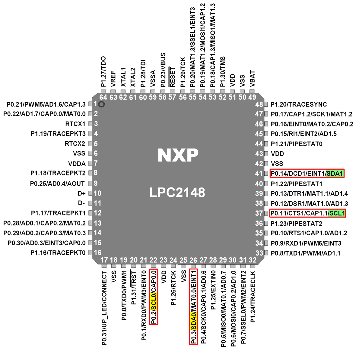
SCL0: - Serial Clock pin of I2C0.
SDA0: - Serial Data pin of I2C0.
SCL1: - Serial Clock pin of I2C1.
SDA1: - Serial Data pin of I2C1.
Let’s see the registers that are used to initialize and control the operation of LPC2148 I2C.
I2C0 and I2C1 have similar register formats and register names. The only difference in their register names is the I2C0 or I2C1 acronym at the beginning of the register name.
Here we will be showing I2C0 registers. Same can be used for I2C1 by changing their name (Replace the I2C0 part by I2C1).
I2C Registers
1. I2C0CONSET (I2C0 Configuration Set Register)
- It is an 8-bit read-write register.
- It is used to control the operation of the I2C0 interface.

- Writing a 1 to a bit in this register causes corresponding bit in the I2C control register to set.
- Writing a 0 has no effect.
- Bit 2 – AA (Assert Acknowledge Flag)
When set to 1, Acknowledge (SDA LOW) is returned during acknowledge clock pulse on SCL. Otherwise, Not acknowledge (SDA HIGH) is returned. - Bit 3 – SI (I2C Interrupt Flag)
This bit is set when the I2C state changes. Else it remains reset. - Bit 4 – STO (Stop Flag)
In Master Mode, setting this bit causes the I2C interface to transmit a STOP condition. In Slave Mode, setting this bit causes recover from an error condition if any.
This bit is cleared by hardware automatically. - Bit 5 – STA (Start Flag)
Setting this bit causes the I2C interface to enter in master mode and transmit a START condition or transmit a repeated START condition if it is already in master mode. - Bit 6 – I2CEN (I2C Interface Enable)
Set this bit to enable I2C interface.
2. I2C0CONCLR (I2C0 Configuration Clear Register)
- It is an 8-bit write only register.
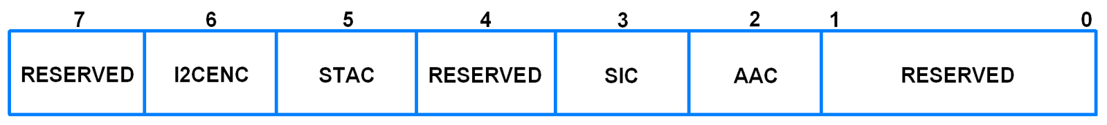
- Writing a 1 to a bit in this register causes corresponding bit in the I2C control register to clear.
- Writing a 0 has no effect.
- Bit 2 – AAC (Assert Acknowledge Flag Clear)
Setting this bit clears the AA bit in I2C0CONSET register. - Bit 3 – SIC (I2C Interrupt Flag Clear)
Setting this bit clears the SI bit in I2C0CONSET register. - Bit 5 – STAC (Start Flag Clear)
Setting this bit clears the STA bit in I2C0CONSET register. - Bit 6 – I2CENC (I2C Interface Disable)
Setting this bit clears the I2CEN bit in I2C0CONSET register.
3. I2C0STAT (I2C0 Status Register)
- It is an 8-bit read only register.
- It reflects the present status of the I2C interface.

- Bit 2:0 – Unused bits
These are unused bits and are always 0. - Bit 7:3 – Status
These are status bits which provide the status of the current event on I2C bus.
There are 26 possible status codes.
Example, I2C0STAT = 0x08. This code indicates that a start condition has been transmitted.
For other status codes, refer Table 232 (Page 228) to table 235 of the datasheet given in the attachments section below.
4. I2C0DAT (I2C0 Data Register)
- It is an 8-bit read-write register.

- It contains the data to be transmitted or received.
- This register can be read or written to only when SI = 1.
5. I2C0SCLL (I2C0 SCL Low Duty Cycle Register)
- It is a 16-bit register.

- This register contains the value for SCL Low time of the cycle.
6. I2C0SCLH (I2C0 SCL High Duty Cycle Register)
- It is a 16-bit register.

- This register contains the value for SCL High time of the cycle.
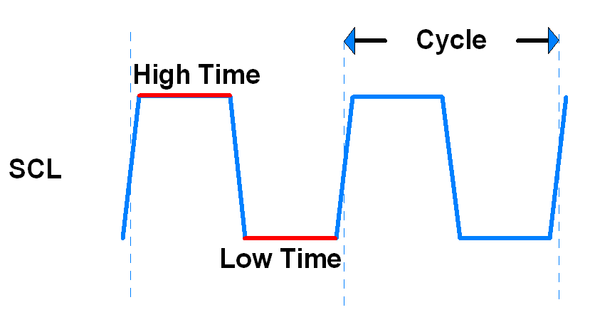
The frequency and duty cycle of SCL is decided using I2C0SCLL and I2C0SCLH. I2C0SCLH contains the TON (High) time and I2C0SCLL contains the TOFF (Low) time.
The frequency is calculated as follows:
Example: Assume FPCLK = 30MHz, I2CBitFrequency = 300KHz, Duty Cycle = 50%.
As duty cycle is 50%, I2C0SCLL = I2C0SCLH.
Hence,
Hence, I2C0SCLL = I2C0SCLH = 50
7. I2C0ADR (I2C0 Slave Address Register)
- It is an 8-bit read-write register.
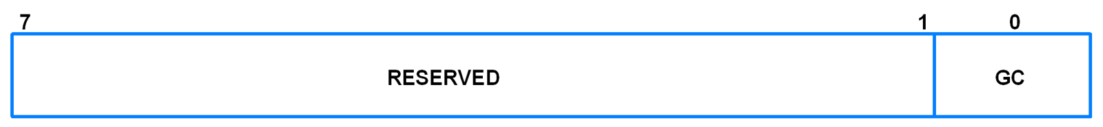
- It is only used when device is in Slave Mode.
- Bit 0 – GC (General Call)
When this bit is set, the general call address (0x00) is recognized. - Bit 7:1 – Address
It contains the I2C device address for slave mode.
Programming I2C0 in LPC2148
We will see how to use I2C0 in master mode to read and write data to and from a slave I2C device.
1. Initialization
- Configure P0.2 and P0.3 as SCL0 and SDA0 using PINSEL0 register.
- Enable I2C interface using the I2C0CONSET register.
- Select appropriate values of I2C0SCLL and I2C0SCLH depending on the duty cycle and frequency of I2C SCL required.
void I2C_INIT(void)
{
	PINSEL0 = PINSEL0 | 0x00000050; /* Configure P0.2 and P0.3 as SCL0 and SDA0 respectively */
	I2C0CONSET = 0x40; /* Enable I2C  */
	I2C0SCLL = 0x32; /* I2C data rate 300Khz and 50% duty cycle */
	I2C0SCLH = 0x32; /* I2C data rate 300Khz and 50% duty cycle */
}
2. Start
- Using I2C0CONSET register, transmit Start condition.
- Wait till SI = 1, i.e. till start condition transmission is completed.
- Clear the Start and SI bits using I2C0CONCLR register.
void I2C_START(void)
{
	I2C0CONSET = 0x20; /* Set Start bit for Start condition */
	while ( (I2C0CONSET & 0x08) == 0 ); /* Wait till SI = 1 */
	I2C0CONCLR = 0x28; /* Clear Start bit and SI bit */
}
3. Write
- Load the data to be written into the data register.
- Enable I2C interface using I2C0CONSET register.
- Wait till SI = 1, i.e. till write complete.
- Clear the SI bit using I2C0CONCLR register.
void I2C_WRITE( char data )
{
	I2C0DAT = data; /* Load data to be written into the data register */
	I2C0CONSET = 0x40; /* Enable I2C */
	while( (I2C0CONSET & 0x08) == 0 ); /* Wait till SI = 1 */
	I2C0CONCLR = 0x08;  /* Clear SI bit */
}
4. Read
- Enable I2C with or without acknowledge depending on whether acknowledge is required.
- Wait till SI = 1, i.e. till reception is complete.
- Clear SI ( and AA if acknowledge is enabled ) bit using I2C0CONCLR register.
- Read the data in the data register.
unsigned char I2C_READ_ACK( void )
{
	I2C0CONSET = 0x44; /* Enable I2C with Acknowledge */
	while( (I2C0CONSET & 0x08) == 0 ); /* Wait till SI = 1 */
	I2C0CONCLR = 0x0C; /* Clear SI and Acknowledge bits */
	return I2C0DAT; /* Return received data */
}
unsigned char I2C_READ_NACK( void )
{
I2C0CONSET = 0x40; /* Enable I2C without Acknowledge */
while( (I2C0CONSET & 0x08) == 0 ); /* Wait till SI = 1 */
I2C0CONCLR = 0x08; /* Clear SI bit */
return I2C0DAT; /* Return received data */
}void I2C_MULTIREAD( char* arr , int bytes ) /* For reading multiple bytes at a time */
{
uint8_t i = 0;
while( ( bytes - 1 ) != 0 )
{
I2C0CONSET = 0x44; /* Enable I2C with Acknowledge */
while( (I2C0CONSET & 0x08) == 0 ); /* Wait till SI = 1 */
I2C0CONCLR = 0x0C; /* Clear SI and Acknowledge bits */
*( arr + i ) = I2C0DAT ;
bytes--;
i++;
}
I2C0CONSET = 0x40; /* Enable I2C without Acknowledge */
while( (I2C0CONSET & 0x08) == 0 ); /* Wait till SI = 1 */
I2C0CONCLR = 0x08; /* Clear SI bit */
*( arr + i ) = I2C0DAT ;
}
5. Stop
- Using I2C0CONSET register, transmit Stop condition.
void I2C_STOP( void )
{
	I2C0CONSET = 0x50; /* Set Stop bit for Stop condition */
}
Components Used |
||
|---|---|---|
| ARM7 LPC2148 ARM7 LPC2148 |
X 1 | |