Introduction to GPIO
General-purpose input/output (GPIO) is a pin on an IC (Integrated Circuit). It can be either input pin or output pin, whose behaviour can be controlled at the run time. A group of these pins is called a port (Example, Port 0 of LPC2148 has 32 pins).
LPC2148 has two 32-bit General Purpose I/O ports.
1. PORT0
2. PORT1
PORT0 is a 32-bit port
- Out of these 32 pins, 28 pins can be configured as either general purpose input or output.
- 1 of these 32 pins (P0.31) can be configured as general-purpose output only.
- 3 of these 32 pins (P0.24, P0.26 and P0.27) are reserved. Hence, they are not available for use. Also, these pins are not mentioned in pin diagram.
PORT1 is also a 32-bit port. Only 16 of these 32 pins (P1.16 – P1.31) are available for use as general-purpose input or output.
ARM LPC2148 Pin Diagram
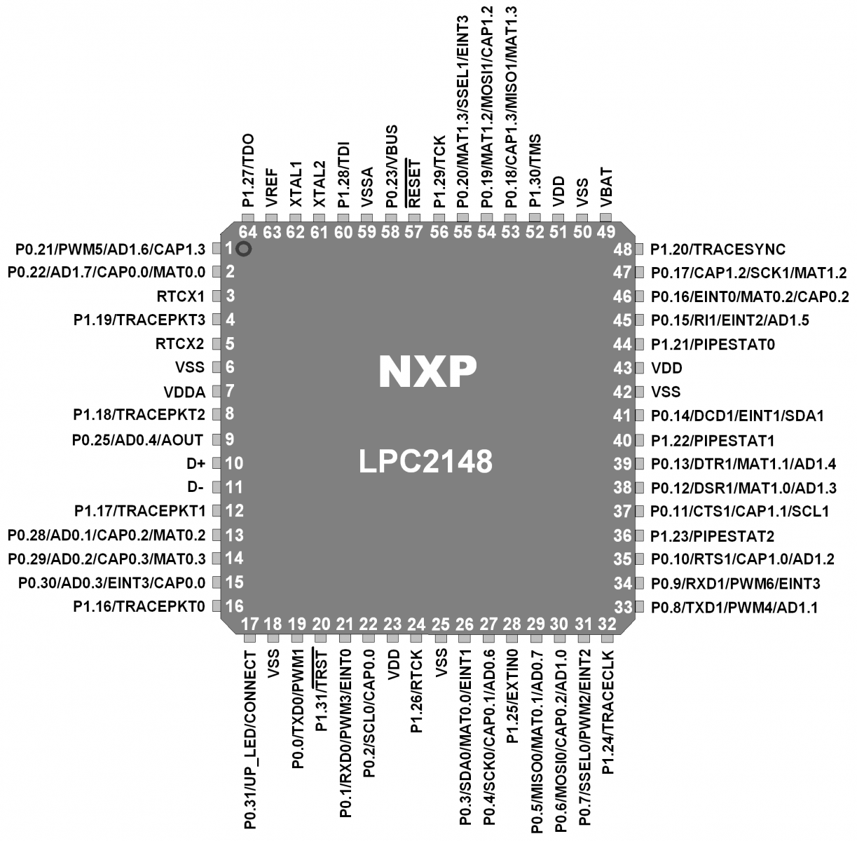
Almost every pin of these two ports has some alternate function available. For example, P0.0 can be configured as the TXD pin for UART0 or as PWM1 pin as well. The functionality of each pin can be selected using the Pin Function Select Registers.
Note : The Port 0 pins do not have built-in pull-up or pull-down resistors. Hence, while using GPIOs on Port 0, in some cases, we need to connect pull-up or pull-down resistors externally.
Pin Function Select Registers
Pin Function Select Registers are 32-bit registers. These registers are used to select or configure specific pin functionality.
There are 3 Pin Function Select Registers in LPC2148:
1. PINSEL0 : - PINSEL0 is used to configure PORT0 pins P0.0 to P0.15.
2. PINSEL1 : - PINSEL1 is used to configure PORT0 pins P0.16 to P0.31.
3. PINSEL2 : - PINSEL2 is used to configure PORT1 pins P1.16 to P1.31.
Let’s see GPIO registers that control the GPIO operations.
Fast and Slow GPIO Registers
There are 5 Fast (also called Enhanced GPIO Features Registers) GPIO Registers and 4 Slow (also called Legacy GPIO Registers) GPIO Registers available to control PORT0 and PORT1.
The Slow Registers allow backward compatibility with earlier family devices using the existing codes.
Slow GPIO Registers
There are 4 Slow GPIO registers :
1. IOxPIN (GPIO Port Pin value register): This is a 32-bit wide register. This register is used to read/write the value on Port (PORT0/PORT1). But care should be taken while writing. Masking should be used to ensure write to the desired pin.
Examples:
a) Writing 1 to P0.4 using IO0PIN
IO0PIN = IO0PIN | (1<<4)b) Writing 0 to P0.4 using IO0PIN
IO0PIN = IO0PIN & (~(1<<4) )c) Writing F to P0.7-P0.4
IO0PIN = IO0PIN | (0x000000F0)
2. IOxSET (GPIO Port Output Set register) : This is a 32-bit wide register. This register is used to make pins of Port (PORT0/PORT1) HIGH. Writing one to specific bit makes that pin HIGH. Writing zero has no effect.
3. IOxDIR (GPIO Port Direction control register) : This is a 32-bit wide register. This register individually controls the direction of each port pin. Setting a bit to ‘1’ configures the corresponding pin as an output pin. Setting a bit to ‘0’ configures the corresponding pin as an input pin.
4. IOxCLR (GPIO Port Output Clear register) : This is a 32-bit wide register. This register is used to make pins of Port LOW. Writing one to specific bit makes that pin LOW. Writing zeroes has no effect.
Examples:
a) Configure pin P0.0 to P0.3 as input pins and P0.4 to P0.7 as output pins.
IO0DIR = 0x000000F0;b) Configure pin P0.4 as an output. Then set that pin HIGH.
	IO0DIR = 0x00000010; OR IO0DIR = (1<<4);
	IO0SET = (1<<4);
c) Configure pin P0.4 as an output. Then set that pin LOW.
	IO0DIR = 0x00000010; OR IO0DIR = (1<<4);
	IO0CLR = (1<<4);
Fast GPIO Registers
There are 5 fast GPIO registers :
1. FIOxDIR (Fast GPIO Port Direction control register) : This is a 32-bit wide register.This register individually controls the direction of each port pin. Setting a bit to ‘1’ configures the corresponding pin as an output pin. Setting a bit to ‘0’ configures the corresponding pin as an input pin.
2. FIOxMASK (Fast Mask register for port) : This is a 32-bit wide register. This register controls the effect of fast registers (FIOxPIN, FIOxSET, FIOxCLR) on port pins. Setting a bit to ‘0’ configures the corresponding pin access to the fast registers i.e. we can write/read the corresponding pin in fast mode using fast registers. Setting a bit to ‘1’ configures the corresponding pin unaffected by fast registers.
3. FIOxPIN (Fast Port Pin value register using FIOMASK) : This is a 32-bit wide register. This register is used to read/write the value on port pins, only if that corresponding port pins have access to fast registers (Access to port pins using fast registers is enabled using Zeroes in FIOxMASK register).
4. FIOxSET (Fast Port Output Set register using FIOMASK) : This is a 32-bit wide register. This register is used to make pins of Port HIGH. Writing one to specific bit makes that pin HIGH. Writing zero has no effect. Reading this register returns the current contents of the port output register. Only bits enabled by ZEROES in FIOMASK can be altered.
5. FIOxCLR (Fast Port Output Clear register using FIOMASK) : This is a 32-bit wide register.This register is used to make pins of Port LOW. Writing one to specific bit makes that pin LOW. Writing zeroes has no effect. Only bits enabled by ZEROES in FIOMASK can be altered.
Aside from the 32-bit long and word only accessible registers mentioned above, every fast GPIO port can also be controlled via several byte and half-word accessible registers. Refer chapter 8 (Page 83) on GPIO in the datasheet of LPC2148 provided in the attachments section for their use.
Examples:
a) Configure pin P0.0 to P0.3 as input pins and P0.4 to P0.7 as output pins.
FIO0DIR = 0x000000F0;b) Configure pin P0.4 as an output. Then set that pin HIGH.
	FIO0DIR = 0x00000010; OR FIO0DIR = (1<<4);
	FIO0SET = (1<<4);
c) Configure pin P0.4 as an output. Then set that pin LOW.
	FIO0DIR = 0x00000010; OR FIO0DIR = (1<<4);
	FIO0CLR = (1<<4);
Why this is called Fast GPIO :
Fast GPIO registers are relocated to the ARM local bus. This makes software access to GPIO pins 3.5 times faster than access through Slow GPIO registers. This effect will not always be visible when a program is written in c code. It may be more evident in an assembly code than in a c code.
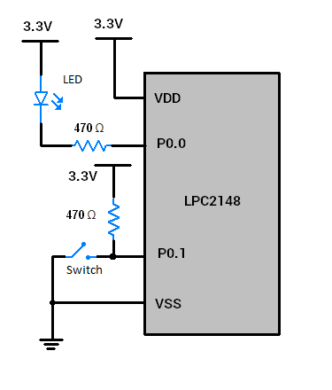
Control LED using Push Button using LPC2148
Now, let’s write a simple program for turning LED ON or OFF depending on the status of the pin.
Here, LED is interfaced to P0.0.
A switch is interfaced to P0.1 to change the status of the pin.
Interfacing Diagram
Program for Control LED using Push Button
/*
  Input-Output Pin Programming to Drive LED through switch
  http://www.electronicwings.com/arm7/lpc2148-32-bit-arm7tdmi-s-processor-gpio-ports-and-registers
*/

#include <lpc214x.h>
#include <stdint.h>

int main(void)
{
	//PINSEL0 = 0x00000000;	/* Configuring P0.0 to P0.15 as GPIO */
	/* No need for this as PINSEL0 reset value is 0x00000000 */
	IO0DIR = 0x00000001;		/* Make P0.0 bit as output bit, P0.1 bit as an input pin  */
	while(1)
	{
		if ( IO0PIN & (1<<1) )	/* If switch is open, pin is HIGH */
		{
			IO0CLR = 0x00000001;  /* Turn on LED */
		}
		else /* If switch is closed, pin is LOW */
		{
			IO0SET = 0x00000001;	/* Turn off LED */
		}
	}
}
Components Used |
||
|---|---|---|
| ARM7 LPC2148 ARM7 LPC2148 |
X 1 | |
| LED 5mm LED 5mm |
X 1 | |
| Mini Push Button Switch - 5-6mm Mini Push Button Switch - 5-6mm |
X 1 | |