Introduction to SPI
The Serial Peripheral Interface (SPI) is a bus interface connection protocol originally started by Motorola Corp.
- SPI Interface uses four wires for communication. Hence it is also known as four wire serial communication protocol.
- SPI is a full duplex master-slave communication protocol. This means that only a single master and a single slave can communicate on the interface bus at the same time.
- SPI enabled devices work in two basic modes of SPI operation i.e. SPI Master Mode and SPI Slave Mode.
- Master Device is responsible for initiation of communication.
- Master Device generates Serial Clock for synchronous data transfer.
- Master Device can handle multiple slave devices on the bus by selecting them one by one.
LPC2148 SPI
- LPC2148 has two inbuilt SPI modules i.e. SPI0 and SPI1/SSP (Synchronous Serial Port).
- SPI0 supports variable (8 to 16) bits of data per transfer.
- SPI0 module is compatible with Motorola SPI (SPI0).
- SSP/SPI1 supports variable (4 to 16) bits of frame.
- SSP/SPI1module is compatible with Motorola SPI (SPI1), Texas Instruments SSI format, National Semiconductor Microwire format bus interface.
LPC2148 SPI Pins
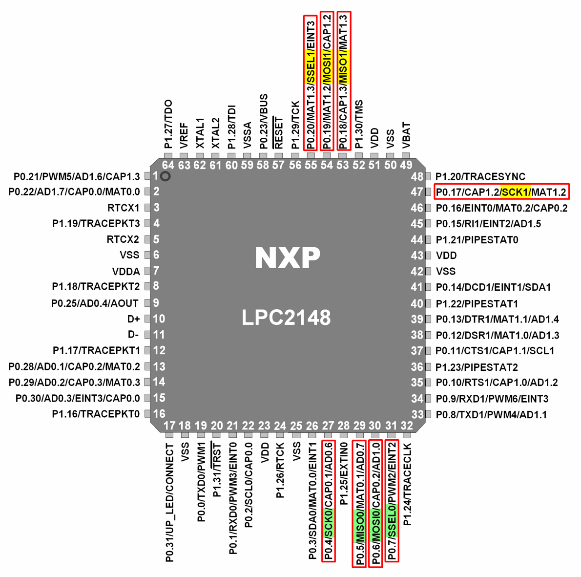
- MISO (Master In Slave Out)
Out from Slave.
Master receives data and slave transmits data through this pin. - MOSI (Master Out Slave In)
Out from Master.
Master transmits data and slave receives data through this pin. - SCK (Serial Clock)
Out from Master.
Master generates this clock for synchronized data transfer.
Only master can initiate serial clock. - SSEL (Slave Select)
Out from Master.
This pin is used by the master to select slave device.
We will see how to use SPI0 here.
We need to initialize SPI0 before using it. Certain registers need to be configured according to our needs.
Let’s see the registers that we will require to use SPI0.
SPI0 Registers
1. S0SPCR (SPI0 Control Register)
- It is a 16-bit register.
- It is a read-write register.
- It is used to control the function of SPI block.
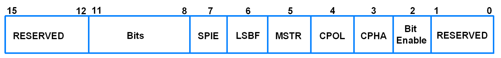
- Bit 2 – Bit Enable
0 = SPI controller sends and receives 8 bits of data per transfer
1 = SPI controller sends and receives the number of bits selected by bits 11:8 - Bit 3 – CPHA (Clock Phase)
0 = Data Sampled on Leading Edge of SCK
1 = Data Sampled on Trailing Edge of SCK - Bit 4 – CPOL (Clock Polarity)
0 = SCK is active high, Leading Edge is Rising
1 = SCK is active low, Leading Edge is Falling - Bit 5 – MSTR (Master Mode Select)
0 = SPI operates in Slave Mode
1 = SPI operates in Master Mode - Bit 6 – LSBF (LSB First)
0 = Data transferred MSB (Bit 7) First
1 = Data transferred LSB (Bit 0) First - Bit 7 – SPIE (Serial Peripheral Interrupt Enable)
0 = SPI Interrupts are disabled
1 = Hardware interrupt generated each time SPIF or WCOL bits are activated - Bit 11:8 – Bits
It decides the number of bits per transfer. Bit2 of this register (Bit Enable) must be 1 for this.
1000 = 8-bits per transfer
1001 = 9-bits per transfer
1010 = 10-bits per transfer
1011 = 11-bits per transfer
1100 = 12-bits per transfer
1101 = 13-bits per transfer
1110 = 14-bits per transfer
1111 = 15-bits per transfer
0000 = 16-bits per transfer
2. S0SPSR (SPI0 Status Register)
- It is an 8-bit register.
- It is a read only register.
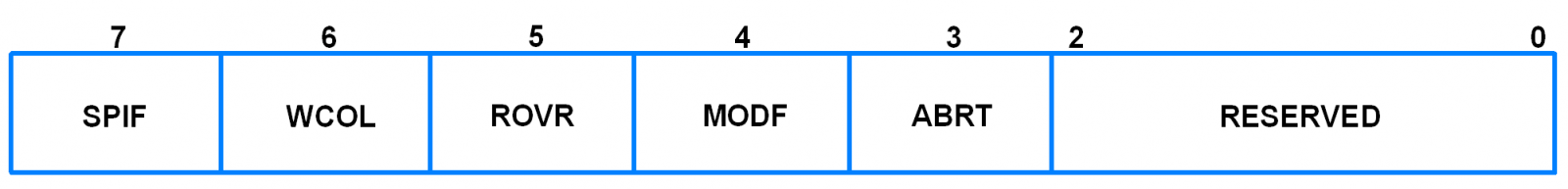
- Bit 3 – ABRT (Slave Abort)
Slave abort happens when slave select pin goes inactive (high) before data transfer is complete.
0 = No slave abort
1 = Slave abort occurred
This bit is cleared by reading the register. - Bit 4 – MODF (Mode Fault)
In SPI Master mode, if SSEL (Slave Select) signal goes active (low), it means that another SPI master has selected this device to be the slave. This condition is known as Mode fault.
0 = No mode fault
1 = Mode fault occurred
This bit is cleared by reading the register, then writing to the SPI control register. - Bit 5 – ROVR (Read Overrun)
When SPI read buffer already contains data to be read and new data is received before available data in the buffer is read, then, new received data will be lost and Read Overrun bit gets set.
0 = No read overrun
1 = Indicates that a read overrun occurred
This bit is cleared by reading the register. - Bit 6 – WCOL (Write Collision)
When SPI data transfer is currently in progress and SPI data register is written with new data before the current transfer is complete, then, write collision is said to have occurred and this bit gets set.
0 = No write collision
1 = Write collision occurred
This bit is cleared by reading the register, then accessing the SPI data register. - Bit 7 – SPIF (SPI Transfer Complete Flag)
0 = SPI transfer not completed yet
1 = SPI transfer completed
This bit is cleared by reading the register, then accessing the SPI data register.
3. S0SPDR (SPI Data Register)
- This is a 16-bit register.
- It is a read-write register.
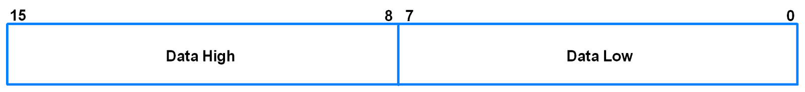
- It holds the data to be transmitted/received.
- Once a data transfer starts, writes to this register are blocked till SPIF becomes 1.
- Bit 7:0 – Data Low
It is lower 8-bit of the data. - Bit 15:8 – Data High
It is higher 8-bit of the data.
This consists the data bits only when there are more than 8-bits of data per transfer.
The number of data bits per transfer is decided by the bits 11:8 in the SPI0 control register.
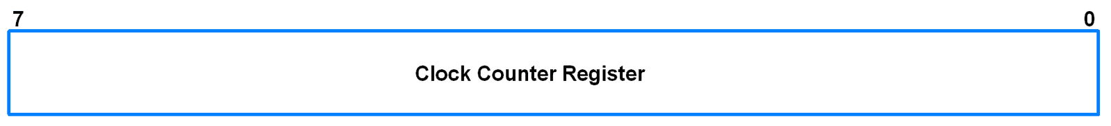
4. S0SPCCR (SPI0 Clock Counter Register)
- This register controls the frequency of master SCK (Serial Clock).
- This is an 8-bit register.
- It indicates the number of PCLK(Peripheral clock) cycles that make up an SPI clock.
- It should always contain an even number which is greater than 8. Violation of this may result in unpredictable behaviour.
5. S0SPINT (SPI0 Interrupt Register)
- It is an 8-bit register.
- It is a read-write register.
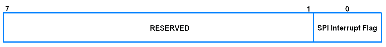
- Bit 0 – SPI Interrupt Flag
It is set by SPI Interface to generate an interrupt.
It is cleared by writing a 1 to it.
This bit will set when SPIE = 1 and either MODF or SPIF bits changes from 0 to 1.
SPI Pin Directions
| SPI Pins | Pin Direction in Master Mode | Pin Direction in Slave Mode |
| MOSI | Output | Input |
| MISO | Input | Output |
| SSEL | Output | Input |
| SCK | Output | Input |
LPC2148 SSP/SPI1
Synchronous Serial Port (SSP) module allows us to use different SPI formats. It includes Motorola, Texas Instruments, and National Semiconductor Microwire SPI bus formats.
All operations & register format are same for SPI0 (explained above) and SSP/SPI1 module except for some minor changes in their register names & some bits described format wise. You can refer SSP module from user manual attached at the end of the document.
Example
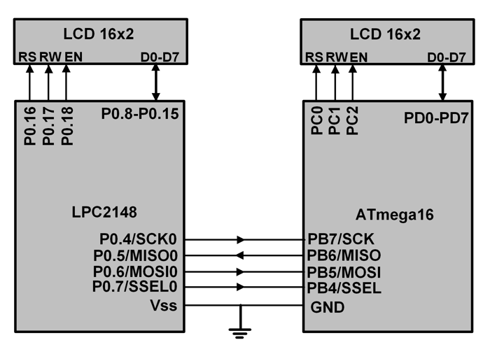
Let’s configure LPC2148 as a Master device and ATmega16 as a slave device. LPC2148 will send an integer that will increment from 0 to 15 to ATmega16. ATmega16 will read the integer and display its value on LCD.
For information about ATmega16 SPI refer this link
Steps for SPI0 Initialization
1. Initialization for Master (LPC2148)
- Using pin select register (PINSEL), configure P0.4, P0.5, P0.6 and P0.7 as SCK0, MISO0, MOSI0 and GPIO respectively. SSEL (P0.7) is configured as general purpose output pin in order to select slave device.
- Using S0SPCR, SPI master mode is selected with 8-bit data and CPOL = CPHA =0. S0SPCR value will change according to configuration required.
- Select clock pre-scalar using S0SPCCR.
void SPI_Master_Init()
{
	PINSEL0 = PINSEL0 | 0x00001500; /* Select P0.4, P0.5, P0.6, P0.7 as SCK0, MISO0, MOSI0 and GPIO */
	S0SPCR = 0x0020; /* SPI Master mode, 8-bit data, SPI0 mode */
	S0SPCCR = 0x10; /* Even number, minimum value 8, pre scalar for SPI Clock */
}
2. Initialization for Slave (ATmega16)
- PB4, PB5, PB6 and PB7 are the SS, MOSI, MISO and SCK pins respectively.
- Using data direction register, configure the MISO pin as output. Also configure MOSI, SS and SCK pins as input pins.
- Enable SPI using SPCR register.
void SPI0_SLAVE_INIT( void )
{
		DDRB = DDRB | (1<<MISO);	/* Make MISO pin output */
		DDRB &= ~( (1<<MOSI) | (1<<SCK) | (1<<SS) );	/* Make MOSI, SCK and SS pins as inputs. */
		SPCR = (1<<SPE);     /* Enable SPI */
}
Steps for SPI0 Data Transfer
1. SPI0 Master Write Mode (LPC2148)
- Make SSEL pin low (we have configured SSEL pin as GPIO to select slave) using IOCLR to select slave.
- Load data to be written into the data register.
- Wait till transmission is completed, i.e. till the SPIF bit becomes 1.
- Make SSEL pin high using IOSET to deselect the slave and to disable SPI transmission to that device.
void SPI_Master_Write(char data)
{
	char flush;
	IO0CLR = (1<<7);  /* SSEL = 0, enable SPI communication with slave */
	S0SPDR = data;  /* Load data to be written into the data register */
	while ( (S0SPSR & 0x80) == 0 );  /* Wait till data transmission is completed */
	flush = S0SPDR;
	IO0SET = (1<<7);  /* SSEL = 1, disable SPI communication with slave */
}
2. SPI0 Master Read Mode (LPC2148)
- Make SSEL pin low (we have configured SSEL pin as GPIO to select slave) using IOCLR to select slave.
- Transmit Flush Byte.
- Wait till data transmission is completed. When data transmission is completed, data sent by slave will be received.
- Make SSEL pin high using IOSET to deselect the slave and to disable SPI transmission to that device.
- Read the data in the data register. This is the received data.
char SPI_Master_Read()
{
	IO0CLR = (1<<7);  /* SSEL = 0, enable SPI communication with slave */
	S0SPDR = 0xFF;  /* Transmit Flush byte */
	while ( (S0SPSR & 0x80) == 0 );  /* Wait till data transmission is completed */
	IO0SET = (1<<7);  /* SSEL = 1, disable SPI communication with slave */
	return S0SPDR;  /* Return the data received */
}
3. SPI Slave Write Mode (ATmega16)
- Load data to be written into the data register.
- Wait till transmission is completed, i.e. till the SPIF bit becomes 1.
void SPI_SLAVE_WRITE_CHAR(char ch)
{
	char flush;
	SPDR = ch; /* Load data to be written into the data register */
	while(!(SPSR & (1<<SPIF))); /* Wait till data transmission is completed */
	flush = SPDR; /* Return the data received */
}
4. SPI Slave Read Mode (ATmega16)
- Wait till SPIF bit becomes 1, i.e. till data reception is completed.
- Read the data in the data register. This is the received data.
unsigned char SPI_SLAVE_READ_CHAR()
{
	while(!(SPSR & (1<<SPIF))); /* Wait till data reception is completed */
	return SPDR;
}
Program for SPI Master (LPC2148)
/*
  LPC2148(ARM7) as master for SPI communication
  http://www.electronicwings.com/arm7/lpc2148-spi-serial-peripheral-interface
*/

#include <lpc214x.h>
#include <stdint.h>
#include <string.h>
#include "LCD-16x2-8bit.h"
#include <stdio.h>

void SPI_Init()
{
	PINSEL0 = PINSEL0 | 0x00001500; /* Select P0.4, P0.5, P0.6, P0.7 as SCK0, MISO0, MOSI0 and GPIO */
	S0SPCR = 0x0020; /* SPI Master mode, 8-bit data, SPI0 mode */
	S0SPCCR = 0x10; /* Even number, minimum value 8, pre scalar for SPI Clock */
}

void SPI_Write(char data)
{
	char flush;
	IO0CLR = (1<<7);  /* SSEL = 0, enable SPI communication with slave */
	S0SPDR = data;  /* Load data to be written into the data register */
	while ( (S0SPSR & 0x80) == 0 );  /* Wait till data transmission is completed */
	flush = S0SPDR;
	IO0SET = (1<<7);  /* SSEL = 1, disable SPI communication with slave */
}

char SPI_Read()
{
	IO0CLR = (1<<7);  /* SSEL = 0, enable SPI communication with slave */
	S0SPDR = 0xFF;  /* Transmit Flush byte */
	while ( (S0SPSR & 0x80) == 0 );  /* Wait till data transmission is completed */
	IO0SET = (1<<7);  /* SSEL = 1, disable SPI communication with slave */
	return S0SPDR;  /* Return the data received */
}

int main(void)
{
	int i,j;
	i = 0;
	j = 0;
	uint16_t rx1;
	char receive, transmit[7];
	memset(transmit,0,7);
	LCD_Init();
	SPI_Init();
	LCD_String("Master send");
	SPI_Write(0x01);
	for(i=0;i<16;i++)
	{
		sprintf(transmit,"i = %d",i);
		while(transmit[j] != 0)
		{
			SPI_Write(transmit[j]);
			delay_ms(100);
			j++;
		}
		SPI_Write('\0');
		LCD_Command(0xC0);
		LCD_String(transmit);
		memset(transmit,0,7);
		j = 0;
	}
	return 0;
}
Program for SPI Slave (ATmega16)
/*
  ATmega16 as slave for SPI communication
  http://www.electronicwings.com/arm7/lpc2148-spi-serial-peripheral-interface
*/

#define F_CPU 8000000UL
#include <avr/io.h>
#include <util/delay.h>
#include <string.h>
#define MOSI PB5
#define MISO PB6
#define SCK PB7
#define SS PB4
#define LCD_PORT PORTD
#define LCD_DATA_PORT_DIRECTION DDRD
#define LCD_COMMAND_PORT PORTC
#define LCD_COMMAND_PORT_DIRECTION DDRC
#define RS PC0
#define RW PC1
#define EN PC2

void LCD_CMD(char command)
{
	LCD_PORT = command;
	LCD_COMMAND_PORT = (0<<RS)|(0<<RW)|(1<<EN);	/* EN = 1, RS = 0, RW = 0 */
	_delay_ms(2);
	LCD_COMMAND_PORT = (0<<RS)|(0<<RW)|(0<<EN);	/* EN = 0, RS = 0, RW = 0 */
	_delay_ms(5);
}

void LCD_INIT(void)
{
	LCD_DATA_PORT_DIRECTION = 0xFF;
	LCD_COMMAND_PORT_DIRECTION = 0xFF;
	_delay_ms(20);
	LCD_CMD(0x38);  /* Initialize lcd */
	LCD_CMD(0x0C);   /* Display on cursor off */
	LCD_CMD(0x06);  /* Auto increment cursor */
	LCD_CMD(0x01);   /* Display clear */
	LCD_CMD(0x80);  /* First line first position */
}

void LCD_STRING (char* msg)
{
	int i=0;
	while(msg[i]!=0)
	{
		LCD_PORT = msg[i];
		LCD_COMMAND_PORT = (1<<RS)|(0<<RW)|(1<<EN);	/* EN = 1, RS = 1, RW = 0 */
		_delay_ms(2);
		LCD_COMMAND_PORT = (1<<RS)|(0<<RW)|(0<<EN);	/* EN = 0, RS = 1, RW = 0 */
		_delay_ms(5);
		i++;
	}
}

void LCD_CHAR (char msg)
{
	LCD_PORT = msg;
	LCD_COMMAND_PORT = (1<<RS)|(0<<RW)|(1<<EN);	/* EN = 1, RS = 1, RW = 0 */
	_delay_ms(2);
	LCD_COMMAND_PORT = (1<<RS)|(0<<RW)|(0<<EN);	/* EN = 0, RS = 1, RW = 0 */
	_delay_ms(5);
}


void SPI0_INIT( void )
{
		DDRB = DDRB | (1<<MISO); /* Make MISO output */
		DDRB &= ~( (1<<MOSI) | (1<<SCK) | (1<<SS) ); /* Make MOSI, SCK and SS pins as inputs. */
		SPCR = (1<<SPE); /* Enable SPI */
}

unsigned char SPI_SLAVE_READ_CHAR()
{
	while(!(SPSR & (1<<SPIF))); /* Wait till data reception is completed */
	return SPDR; /* Return the data received */
}

void SPI_SLAVE_WRITE_CHAR(char ch)
{
	char flush;
	SPDR = ch; /* Load data to be written into the data register */
	while(!(SPSR & (1<<SPIF))); /* Wait till data transmission is completed */
	flush = SPDR;
}


int main(void)
{
	int i = 0;
	int j = 0;
	int k = 0;
	unsigned char receive[7], rx;
	SPI0_INIT();
	LCD_INIT();
	LCD_STRING("Slave receive");
	memset(receive,0,7);
	while(SPI_SLAVE_READ_CHAR() != 0x01);
	do
	{
		do
		{
			receive[j] = SPI_SLAVE_READ_CHAR();
			rx = receive[j];
			j++;
		} while (rx != 0);
		LCD_CMD(0xC0);
		for(i=0;i<j-1;i++)
		LCD_CHAR(receive[i]);
		memset(receive,0,7);
		j = 0;
	} while (k != 16);
	return 0;
}
Video
Components Used |
||
|---|---|---|
| ARM7 LPC2148 ARM7 LPC2148 |
X 1 | |
| LCD16x2 Display LCD16x2 Display |
X 2 | |
| ATmega 16 ATmega 16 |
X 1 | |
| Breadboard Breadboard |
X 1 | |