Introduction
LPC2148 has inbuilt 32-bit timers which count the peripheral clock.
- Compare any value with Timer Counter (TC) value is one feature available in LPC2148 timers. It’s the same as Alarm watch in which we can set any future time to sound an alarm when it matches the watch time.
- LPC2148 compare match works in a similar way but with different functionality on match occurrence.
- We can make specific pins (also called as match pins) of LPC2148 High/Low/Toggle on the event match occurrence.
- We can set any 32-bit timer value at which we want to make High/Low/Toggle corresponding match pin.
- This 32-bit value is written in Match Register (MR) and continuously compared with 32-bit Timer Counter (TC) value.
- When this match register value and Timer Counter (TC) value are equal, we can reset/stop Timer Counter (TC) and can generate an interrupt.
- Timer counter (TC) counts the input PCLK (Peripheral Clock) i.e. one count of Timer Counter (TC) is equal to the one cycle of PCLK
- We can also extend one count of Timer Counter by several PCLK clocks using the Prescale Counter (PC). Prescale Register (PR) is used to set the maximum value for PC.
- PC counts the PCLK clocks up to the maximum value in PR and then resets back to 0.
Now using this scenario, if we reset the Timer Counter at match event occurrence and toggle corresponding match pin, then we can generate square wave on that pin as shown in below figure.
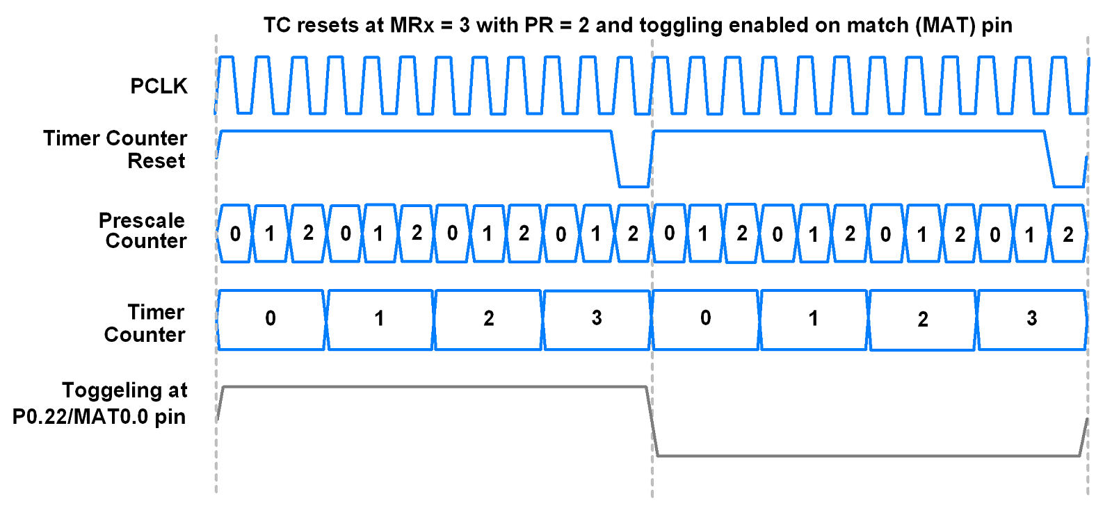
We can generate different square waves with varying frequencies and duty cycles using different match values.
LPC2148 Match Pins
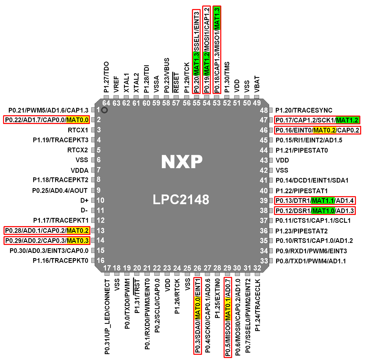
- MAT0.0 (2 pins): P0.3 and P0.22
- MAT0.1 (1 pin): P0.5
- MAT0.2 (2 pin): P0.16 and P0.28
- MAT0.3 (1 pin): P0.29
- MAT1.0 (1 pin): P0.12
- MAT1.1 (1 pin): P0.13
- MAT1.2 (2 pins): P0.17 and P0.19
- MAT1.3 (2 pins): P0.18 and P0.20
Let’s take a quick look at the LPC2148 timer0 registers that are needed for compare operation. Timer0 and timer1 registers are similar in their operation and have similar structures, but differ in names.
Timer0 Registers
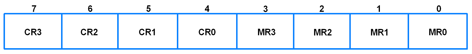
1. T0IR (Timer0 Interrupt Register)
- It is an 8-bit read-write register.
- Consists of 4 bits for match register interrupts and 4 bits for compare register interrupts.
- If interrupt is generated, then the corresponding bit in this register will be high, otherwise it will be low.
- Writing a 1 to any bit of this register will reset that interrupt. Writing a 0 has no effect.
2. T0TCR (Timer0 Timer Control Register)
- It is an 8-bit read-write register.
- It is used to control the operation of the timer counter.

- Bit 0 – Counter Enable
0 = Counters are disabled
1 = Timer counter and Prescale counter are enabled for counting - Bit 1 – Counter Reset
0 = Counter not reset
1 = Timer counter and Prescale counter are synchronously reset on next positive edge of PCLK
3. T0CTCR (Timer0 Counter Control Register)
- It is an 8-bit read-write register.
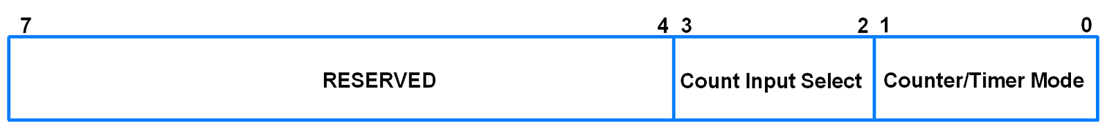
- Used to select between timer or counter mode.
- When in counter mode, it is used to select the pin and edges for counting.
- Bits 1:0 – Counter/Timer Mode
This field selects which PCLK edge can increment Timer’s Prescale Counter (PC), or clear PC and increment Timer Counter (TC).
00 = Timer Mode: Every rising edge of PCLK
01 = Counter Mode: TC is incremented on rising edge on the capture input selected by Bits 3:2
10 = Counter Mode: TC is incremented on falling edge on the capture input selected by Bits 3:2
01 = Counter Mode: TC is incremented on both edges on the capture input selected by Bits 3:2 - Bits 3:2 – Count Input Select
When bits 1:0 in this register are not 00, these bits select which capture pin is sampled for clocking.
00 = CAP0.0
01 = CAP0.1
10 = CAP0.2
11 = CAP0.3 - Note : If the counter mode is selected for a certain capture (CAP) input, then the corresponding 3 bits in the T0CCR register must be programmed as 000. Capture and/or interrupt can be selected for other CAP inputs.
4. T0TC (Timer0 Timer Counter)
- It is a 32-bit timer counter.
- It is incremented when the Prescale Counter (PC) reaches its maximum value held by Prescaler Register (PR).
- Note: When TC overflow occurs, it does not generate any overflow interrupt. Alternatively, we can use match register to detect overflow event if needed.
5. T0PR (Timer0 Prescale Register)
- It is a 32-bit register.
- It holds the maximum value of the Prescale Counter.
6. T0PC (Timer0 Prescale Counter Register)
- It is a 32-bit register.
- It controls the division of PCLK by some constant value before it is applied to the Timer Counter.
- It is incremented on every PCLK.
- When it reaches the value in Prescale Register, the Timer Counter is incremented and Prescale Counter is reset on next PCLK.
7. Match Registers (MR0 – MR3)
- The Match Register (MR) values are continuously compared to the Timer Counter (TC) value.
- When these two values are equal, actions can be triggered automatically.
- Actions are reset the timer, stop the timer, generate an interrupt; and are controlled through Match Control Register.
8. T0MCR (Timer0 Match Control Register)
- It is a 16-bit register.
- It controls what action is to be taken on a match between the Match Registers and Timer Counter.
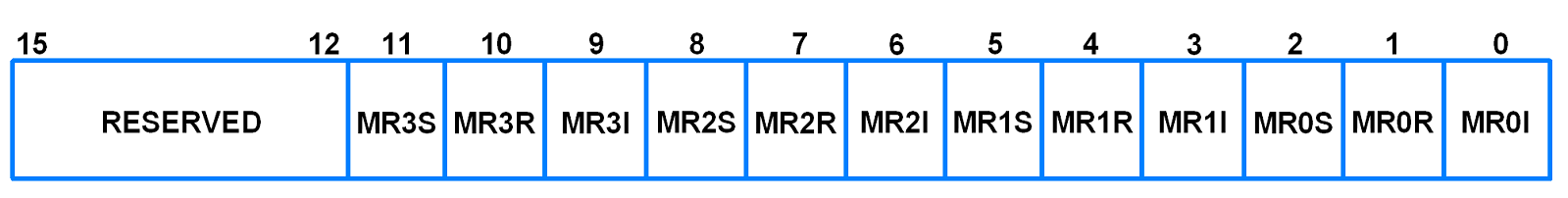
- Bit 0 – MR0I (Match register 0 interrupt)
0 = This interrupt is disabled
1 = Interrupt on MR0. An interrupt is generated when MR0 matches the value in TC (Timer Counter) - Bit 1 – MR0R (Match register 0 reset)
0 = This feature is disabled
1 = Reset on MR0. The TC (Timer Counter) will be reset if MR0 matches it - Bit 2 – MR0S (Match register 0 stop)
0 = This feature is disabled
1 = Stop on MR0. The TC (Timer Counter) and PC (Prescale Counter) is stopped and Counter Enable bit in T0TCR is set to 0 if MR0 matches TC - MR1, MR2 and MR3 bits function in the same manner as MR0 bits.
9. T0EMR (Timer0 External Match Register)
- It is a 16-bit register.
- It provides both control and status of external match pins.
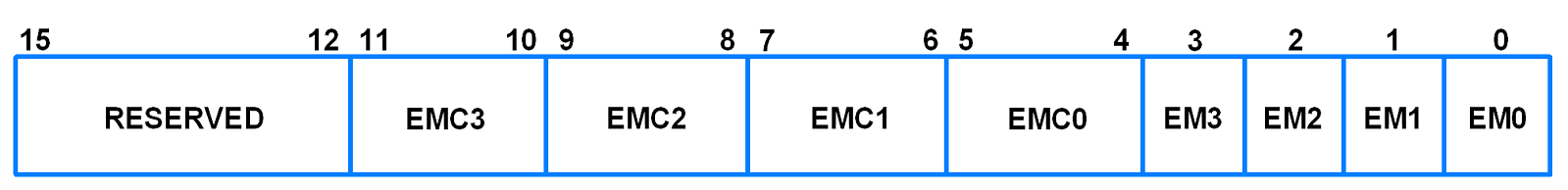
- Bit 0 – EM0 (External Match 0)
This bit reflects the state of output MAT0.0.
When a match occurs between MR0 and TC, this output of timer can toggle, set, clear or do nothing depending upon EMC0 bits. - Bit 5:4 – EMC0 (External Match Control 0)
Determines the functionality of External Match 0.
00 = Do nothing
01 = Clear MAT0.0
10 = Set MAT0.0
11 = Toggle MAT0.0 - EM1, EM2, EM3, EMC1, EMC2 and EMC3 function similar to what is described above for EM0 and EMC0 respectively.
Example
Let’s write a code for generating a square wave of 5Hz with a duty cycle of 50%.
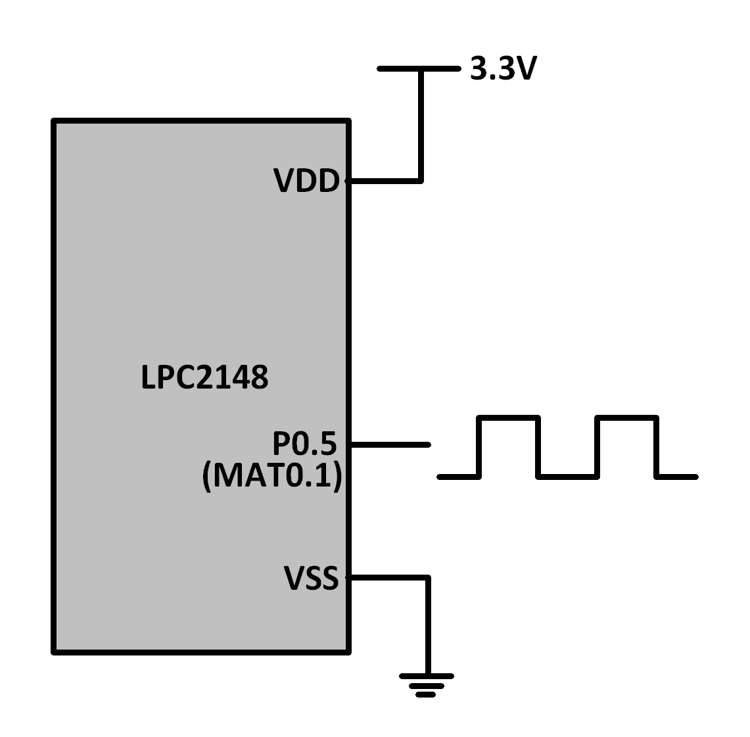
We are using P0.5 as MAT0.1.
The code is similar to the one for delay generation. Only additional part is to use MAT0.1 pin for waveform generation.
Since we are generating a wave with duty cycle of 50%, we are using MAT0.1 in toggle mode.
For waves with different duty cycles, we can configure MAT0.1 to set and clear with appropriate delays according to duty cycle requirement in an alternating manner.
The frequency is also controlled by the value in the match register.
Program for Compare match mode using LPC2148
/*
  Compare match mode for timer in LPC2148(ARM7)
  http://www.electronicwings.com/arm7/lpc2148-resetstop-timer-on-compare-match
*/

#include <lpc214x.h>

__irq void T0_ISR (void)
{
	T0IR = ( T0IR | (0x02) );
	VICVectAddr = 0x00;
}


int main (void)
{
	VPBDIV = 0x00000002; /* For Pclk = 30MHz */
	/* We have configured Cclk=60MHz. Above instruction makes Pclk = Cclk/2 = 30MHz */
	PINSEL0 = PINSEL0 | 0x00000800; /* Configure P0.5 as Match 0.1 */
	VICVectAddr0 = (unsigned) T0_ISR; /* T0 ISR Address */
	VICVectCntl0 = 0x00000024; /* Enable T0 IRQ slot */
	VICIntEnable = 0x00000010; /* Enable T0 interrupt */
	VICIntSelect = 0x00000000; /* T0 configured as IRQ */
	T0TCR = 0x02; /* Reset TC and PR */
	T0CTCR = 0x00; /* Timer mode, increment on every rising edge */
	T0PR = 0x1D; /* Load Pre-Scalar counter with 29 (0 to 29 = 30), so that timer counts every 1usec */
	T0MR1 = 100000; /* Load timer counter for 100msec delay, 1usec*1000*100 */
	T0MCR = 0x0018; /* Interrupt generate on match and reset timer */
	T0EMR = 0x00C0; /* EM1 enable with toggling on match */
	T0TCR = 0x01; /* Enable timer */

	while (1);
}
Video
Components Used |
||
|---|---|---|
| ARM7 LPC2148 ARM7 LPC2148 |
X 1 | |