Introduction Analog to Digital Converter
- When we interface sensors to the microcontroller, the output of the sensor many of the times is analog in nature. But microcontroller processes digital signals.
- Hence we use ADC in between sensors and microcontrollers. It converts an analog signal into digital and gives it to the microcontroller.
- There are a large number of applications of ADC like in a biometric application, Environment monitoring, Gas leakage detection, etc.
So now let’s see ADC in PIC18F4550.
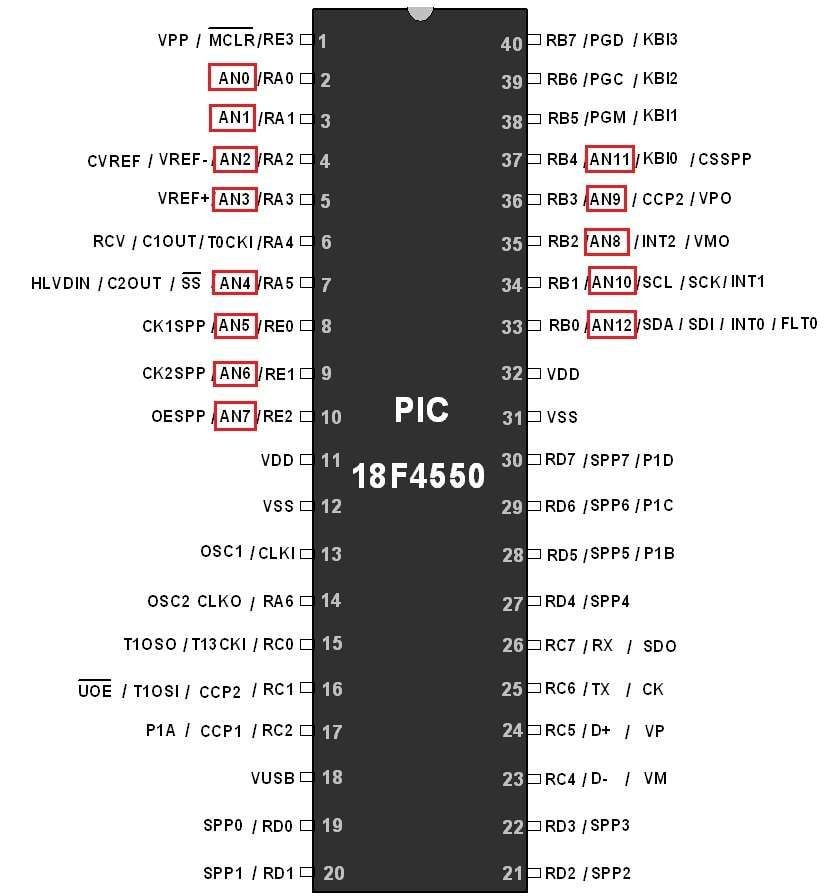
- PIC18f4550 has inbuilt 10-bit 13 channel ADC.
- 13-channels of ADC are named as AN0-AN12. It means we can connect 13 different sensors at the same time.
- 10-bit ADC means:
- It will give digital count in the range of 0-1023 (2^10).
Digital Output value Calculation
- To keep things simple, let us consider that Vref is 5V,
For 0Vin digital o/p value = 0
For 5Vin digital o/p value = 1023 (10-bit)
For 2.5Vin digital o/p value = 512 (10-bit)
PIC18F4550 ADC Pins
ADC Registers of PIC18F4550
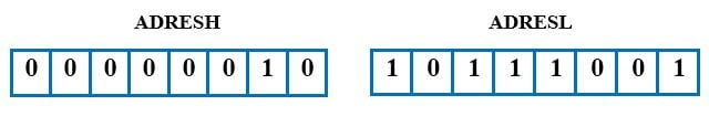
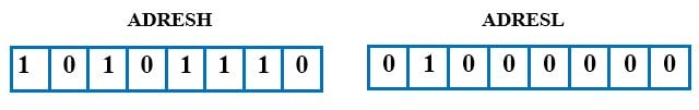
ADRESH (High byte) and ADRESL (Low byte) Registers are used in combination to store the converted data i.e. digital data. But the data is only 10-bit wide, so the remaining six bits are not used.
ADCON0: A/D Control Register 0
CHS3:CHS0: Analog Channel Select Bits
| CHS3:CHS0 | Channels | Channel Name |
| 0000 | Channel 0 | AN0 |
| 0001 | Channel 1 | AN1 |
| 0010 | Channel 2 | AN2 |
| 0011 | Channel 3 | AN3 |
| 0100 | Channel 4 | AN4 |
| 0101 | Channel 5 | AN5 |
| 0110 | Channel 6 | AN6 |
| 0111 | Channel 7 | AN7 |
| 1000 | Channel 8 | AN8 |
| 1001 | Channel 9 | AN9 |
| 1010 | Channel 10 | AN10 |
| 1011 | Channel 11 | AN11 |
| 1100 | Channel 12 | AN12 |
GO/DONE’: A/D Conversion Status Bit
When ADON=1
1= A/D conversion is in progress
0= A/D is idle
ADON: A/D Conversion Enable/ON bit
1= A/D conversion is ON (Start conversion).
0= A/D conversion is disabled.
ADCON1: A/D Control Register 1
VCFG1: Voltage Reference Configuration bit
1= Vref –
0= Vss
VCFG0: Voltage Reference Configuration bit
1= Vref +
0= Vdd
PCFG3:PCFG0: A/D Port Configuration Bits:
As the ADC pins in PIC18F4550 are multiplexed with many other functions. So these bits are used to de-multiplex them and use them as an analog input pin.
.jpg)
ADCON2: A/D Control Register 2
ADCS2:ADCS0: A/D clock conversion select bits:
These bits are used to assign a clock to ADC.
111= FRC Clock derived from A/D RC oscillator
110= FOSC/64
101= FOSC/16
100= FOSC/4
011= FRC Clock derived from A/D RC oscillator
010= FOSC/32
001= FOSC/8
000= FOSC/2
ADFM: A/D Result format select bit:
The 10-bit result will be placed in ADRESH (8-bit) and ADRESL (8-bit).
Consider 10-bit data as follows:

1 = Right Justified. However, the lower 8-bits are kept in ADRESL, and the remaining MSB side two bits kept in ADRESH. And remaining 6 bits (bit 2-7) of ADRESH filled with 0’s.
0 = Left Justified. However, the upper 8-bits are kept in ADRESH, and the remaining two lower bits are placed in ADRESL at bit 7-6 location. And the remaining 6 lower bits of ADRESL filled with 0’s.
ACQT2:ACQT0: A/D Acquisition Time Select Bits:
User can program acquisition time.
Following is the minimum wait time before the next acquisition can be started.
TAD = (A/D Acquisition Time)
000= 0 TAD. Default Acquisition Time for A-D conversion.
001= 2 TAD
010= 4 TAD
011= 6 TAD
100= 8 TAD
101= 12 TAD
110= 16 TAD
111= 20 TAD
Steps for Programming A/D Conversion
Initialization
- Configure ADCON1 Register to select Reference voltage using VCFG1: VCFG0 bits and also configure port pins which we require as an analog input using PCFG3: PCFG0 bits.
- Configure ADCON2 Register to select A/D result format, A/D clock, and acquisition time.
void ADC_Init()
{
    TRISA = 0xFF;	/* Set as input port */
    ADCON1 = 0x0E;	/* Ref vtg is VDD and Configure pin as analog pin */
    ADCON2 = 0x92;	/* Right Justified, 4Tad and Fosc/32. */
    ADRESH=0;		/* Flush ADC output Register */
    ADRESL=0;
}
A/D conversion and Read digital values
- Configure ADCON0 Register to select a channel that we require using CHS3: CHS0.
- Start A/D conversion by setting ADON bit and Go/done’ bit of ADCON0 Register.
- Wait for G0/done’ bit which is cleared when the conversion is completed.
- Then copy Digital data which is stored in ADRESH and ADRESL Register.
int ADC_Read(int channel)
{
    int digital;

    /* Channel 0 is selected i.e.(CHS3CHS2CHS1CHS0=0000) & ADC is disabled */
    ADCON0 =(ADCON0 & 0b11000011)|((channel<<2) & 0b00111100);

    ADCON0 |= ((1<<ADON)|(1<<GO));	/*Enable ADC and start conversion*/

    /* Wait for End of conversion i.e. Go/done'=0 conversion completed */
    while(ADCON0bits.GO_nDONE==1);

    digital = (ADRESH*256) | (ADRESL);	/*Combine 8-bit LSB and 2-bit MSB*/
    return(digital);
}
Application
- Here we are going to develop a short application using the internal ADC of PIC18f4550.
- In this, we will interface a 1K potentiometer which is used to vary the voltage.
- This varying voltage is applied to AN0 (channel 0) of ADC and displays this value on 16x2 LCD.
Interfacing Diagram
.JPG)
PIC18F4550 ADC Program
#include <stdio.h>
#include <string.h>
#include <stdlib.h>
#include <P18F4550.h>
#include "config_intosc.h"	/* Header File for Configuration bits */
#include "LCD_8bit_file.h"	/* Header File for LCD Functions */

void ADC_Init();
int ADC_Read(int);

#define vref 5.00		/* Reference Voltage is 5V*/
void main()
{
    char data[10];
    int digital;
    float voltage;
    OSCCON=0x72;		/*Set internal Osc. frequency to 8 MHz*/
    LCD_Init();			/*Initialize 16x2 LCD*/
    ADC_Init();			/*Initialize 10-bit ADC*/

    LCD_String_xy(1,1,"Voltage is...");

    while(1)
    {
        digital=ADC_Read(0);

	/*Convert digital value into analog voltage*/
        voltage= digital*((float)vref/(float)1023);

	/*It is used to convert integer value to ASCII string*/
        sprintf(data,"%.2f",voltage);

        strcat(data," V");	/*Concatenate result and unit to print*/
        LCD_String_xy(2,4,data);/*Send string data for printing*/
    }

}

void ADC_Init()
{
    TRISA = 0xff;		/*Set as input port*/
    ADCON1 = 0x0e;  		/*Ref vtg is VDD & Configure pin as analog pin*/
    ADCON2 = 0x92;  		/*Right Justified, 4Tad and Fosc/32. */
    ADRESH=0;  			/*Flush ADC output Register*/
    ADRESL=0;
}

int ADC_Read(int channel)
{
    int digital;
    ADCON0 =(ADCON0 & 0b11000011)|((channel<<2) & 0b00111100);

    /*channel 0 is selected i.e.(CHS3CHS2CHS1CHS0=0000)& ADC is disabled*/
    ADCON0 |= ((1<<ADON)|(1<<GO));/*Enable ADC and start conversion*/

    /*wait for End of conversion i.e. Go/done'=0 conversion completed*/
    while(ADCON0bits.GO_nDONE==1);

    digital = (ADRESH*256) | (ADRESL);/*Combine 8-bit LSB and 2-bit MSB*/
    return(digital);
}
Video
Components Used |
||
|---|---|---|
| PIC18f4550 PIC18f4550 |
X 1 | |
| LCD16x2 Display LCD16x2 Display |
X 1 | |
| PICKit 4 MPLAB PICKit 4 MPLAB |
X 1 | |