Introduction
- AVR ATmega16 has 32 pins constituting four ports. The ports are listed below :
1. PORT A
2. PORT B
3. PORT C
4. PORT D. - Each port has 8 pins.
- The pins of these four ports can be used as general-purpose inputs/outputs.
- These pins can be configured as input or output using the three I/O registers for each port. These registers are listed below :
1. DDRxregisters: These are used to decide the direction of the pins, i.e. whether the pins will act as input pins or as output pins
2. PINxregisters: These are used to read the logic level on the port pins.
3. PORTxregisters: These are used to set the logic on the pins HIGH or LOW.
(Where x can be A, B, C, or D depending on which port registers are being addressed). - Each pin also has some special functionality associated with it as well.
The pin diagram of ATmega16/32 is shown in the figure below. The four ports, their pins, and the special functions associated with each pin can be seen in the figure.
I/O Port Registers
There are three I/O registers associated with each port. These are as follows:
- Data register PORTx
- Data direction register DDRx
- Input pins address register PINx
Where x can be A, B, C, or D depending on which port is being addressed.
DDRx: Data Direction Registers
- These are 8-bit registers.
- These are used to configure the pins of the ports as input or output.
- Writing a one to the bits in this register sets those specific pins as output pins.
- Writing a zero to the bits in this register sets those specific pins as input pins.
- All bits in these registers can be read as well as written to.
- The initial value of these bits is zero.
Example :
- Setting Port D as an output port :
DDRD = 0xFF;Writing 1 to the bits of this register configures the pins corresponding to those pins as output pins.
Here we have configured all 8 pins of Port D as output pins by writing 1 to each of them. ( 0xFF = 0b11111111).
- Setting Port D as an input port :
DDRD = 0x00;Writing 0 to the bits of this register configures the pins corresponding to those pins as output pins.
Here we have configured all 8 pins of Port D as input pins by writing 0 to each of them. ( 0x00 = 0b00000000).
PORTx: Data Registers
- These are 8-bit registers.
- These are used to put the pins of the ports in a logic HIGH or logic LOW state.
- Writing a one to the bits in this register puts a HIGH logic (5V) on those pins.
- Whereas writing a zero to the bits in this register puts a LOW logic (0V) on those pins.
- All bits in these registers can be read as well as written to.
- The initial value of these bits is zero.
Example:
We will use the PORTx register of Port D to write a value 0x55 to Port D.
PORTD = 0x55;
PINx: Input Pins Address Registers
- These are 8-bit registers.
- These are used to read the values on the specific pins of the port.
- These bits are read-only bits and cannot be written to.
Example:
We will read the value on Port D in an 8-bit variable named ‘port_value’.
port_value = PIND;
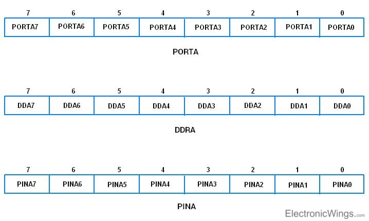
In the figure shown below, the above mentioned three registers for PortA are shown. These are 8-bit registers.
Now let’s see examples of how to program a pin as an input pin and an output pin.
Blink LED Using ATmega16/32
Let’s write a code to program pin 3 of Port D as an output pin and use it to drive an LED. We will toggle the LED with some delay.
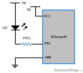
As shown in the above figure, the LED is connected to pin 3 of Port D. The anode of the LED is connected to 5V.
Most of the LEDs require around 10mA current to glow properly.
If the current greater than the maximum rated current of the LED flows through it, the LED will get permanently damaged.
The maximum current rating for LEDs is usually around 20-30mA. Refer to the datasheet of the LED you are using for this rating.
In order to limit the current flowing through the LED, we connect a resistor in series with it.
Assuming that the LED has a 0.7V forward voltage drop and that 10mA current is sufficient for the LED to glow properly, the value of resistance required can be calculated as follows:
Therefore,
The nearest standard value of resistor available is 470Ω. So, that value is used in the circuit.
Program for LED Blinking using ATmega16/32
/*
Output Pin Programming to Drive LED
www.electronicwings.com
 */

#define F_CPU 8000000UL
#include <avr/io.h>
#include <util/delay.h>

int main(void)
{
	DDRD = 0xFF;			/* Making all 8 pins of Port D as output pins */
    /*
    In order to make only PD3 as output while keeping direction of other pins as it is, do the following
    DDRD = DDRD | (1<<3);
    This is equivalent to writing one to only PD3 while keeping the other pins unchanged
    */
    while(1)
    {
        PORTD = PORTD | (1<<3);		/* Making PD3 high. This will make LED ON */
        _delay_ms(100);
        PORTD = PORTD & (~(1<<3));	/* Making PD3 low. This will make LED OFF */
        _delay_ms(100);
        /* Do not keep very small delay values. Very small delay will lead to LED appearing continuously ON due to persistence of vision */
    }
	return 0;
}
LED control with push button using ATmega16/32
Let’s write a code to read the status of the pin as input. We will indicate this status on the LED.
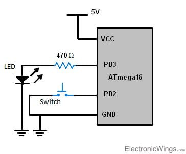
In this example,
- We are using a switch as an input. The switch is connected to PD2 of the controller.
- We are using LED as an indicator of the status of pin PD2. LED is connected to PD3.
Note :
- ATmega16 has internal pull-ups. We can activate it to make pin status HIGH.
- In this code, we will be showing the status of the pin on the LED. We will not be showing the status of the switch on the LED.
When the switch is open, the pin is HIGH, LED will be ON.
When the switch is pressed, the pin is LOW, LED will be OFF.
LED control with push button using ATmega16/32 Program
/*
	ATmega16/32 GPIO Input Pin Programming
	www.electronicwings.com
 */

#define F_CPU 8000000UL
#include <avr/io.h>
#include <util/delay.h>

int main(void)
{
    DDRD = DDRD | (1<<3);		/* Make PD3 as output pin */
    DDRD = DDRD & (~(1<<2));		/* Make PD2 as input pin */
    PORTD = PORTD | (1<<2);		/* Enable pull-up on PD2 by writing 1 to it */
    int pin_status;
    while(1)
    {
        pin_status = PIND & (1<<2);	/*Read status of pin PD2 */
        if(pin_status)			/* Transmit status of pin PD2 on to pin PD3 to drive LED. */
        {
           PORTD = PORTD | (1<<3);	/* Switch is open, pin_status = 1, LED is ON */
        }
        else
        {
           PORTD = PORTD & (~(1<<3));	/* Switch is closed, pin_status = 0, LED is OFF */
        }
    }
    return 0;
}
Understanding I/O pins
All port pins have individually selectable pull-up resistors with resistance which is independent of the supply voltage. All pins have protection diodes to both VCC and Ground.
The equivalent schematic of each I/O pin is shown in the figure below.
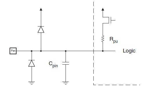
(Image Source: ATmega16 Datasheet)
Current sinking and sourcing
- Each I/O pin can sink or source a maximum current of 40mA.
- Although each pin can sink or source 40mA current, it must be ensured that the current sourced or sunk from all the ports combined, should not exceed 200mA.
- There are further restrictions on the amount of current sourced or sank by each port. For information on this, refer to page 292 in the datasheet of ATmega16 given in the attachments section of this topic.
Pin States
- A port pin can have four different states depending upon the state of the bits corresponding to this pin in the data direction register (DDRx) and a data register (PORTx) of that specific port.
| DDxn | PORTxn | I/O | Pull-Up | Comment |
| 0 | 0 | I | No | Tri-State (High Z) |
| 0 | 1 | I | Yes | Pxn will source current if pulled low externally |
| 1 | 0 | O | No | Output Low (Sink) |
| 1 | 1 | O | No | Output High (Source) |
x is Port and can be A, B, C or D n is Pin number of the Port, and can be 0, 1, 2, 3, 4, 5, 6 or 7 | ||||
- As discussed in the equivalent schematic of I/O pins, each port pin has an internal pull-up resistor. This internal pull-up resistor to all the pins can be disabled by writing one to the PUD bit in the SFIOR register. When this is done, the pins are in tri-state (High impedance states) if DDRxn = 0 and PORTxn = 1.
Precautions to be taken while configuring I/O
- When configuring pins as output pins with HIGH logic, make sure that the pin is not directly connected to the ground.
- When configuring pins as output pins with LOW logic, make sure that the pin is not directly connected to Vcc.
- When configuring pins as input pins, the internal pull-up structure must be kept in mind and connections should be made accordingly. For example, consider a switch as an input to a microcontroller pin. There are two ways to interface the switch as shown below :
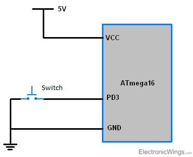
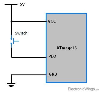
As the pin is configured as an input pin with pull-up activated, connecting the switch as shown in method 2 will not give us the correct status of the switch.
Connecting the switch as shown in method 1 will give us the correct status of the switch.
Components Used |
||
|---|---|---|
| ATmega 16 ATmega 16 |
X 1 | |
| Atmega32 Atmega32 |
X 1 | |
| LED 5mm LED 5mm |
X 1 | |
| Mini Push Button Switch - 5-6mm Mini Push Button Switch - 5-6mm |
X 1 | |