
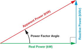
Power Triangle:
For phase angle calculation,
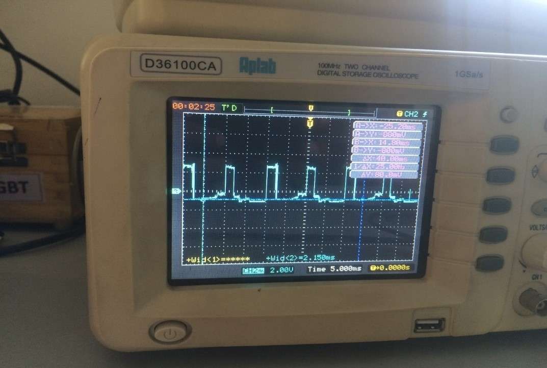
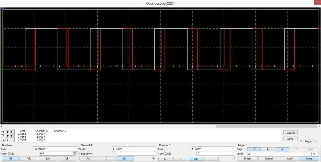
ɸ = Δt x f x 360˚
Where Δt = Time difference (s)
F = Frequency (50 hz)
Power factor = cos ɸ
Power Factor Correction:
Power factor correction is the process of compensating for the lagging current by creating a leading current by connecting capacitor to the supply. A sufficient capacitance can be connected so that the power factor is adjusted to be as close to unity as possible. Power factor correction (PFC) is a system of counteracting the undesirable effects of electric loads that create a power factor that is less than one (1).
In Power factor correction, System scans the current and voltage waveforms of Load connected to Supply OUT at every 10 Seconds. If load having PF less than 0.95 or greater than -0.95, then it considered as Inductive load. As soon as Inductive load detected, Correction Capacitor get added in parallel to Inductive load. (At ideal condition, PF value -1 or +1 considered as Resistive load.)
PROJECT IMPLEMENTATION:
The current and voltage signal are acquired from the main AC line by using Current Transformer and Potential Transformer. These acquired signals are then pass on the Zero crossing detectors. Bridge Rectifier for both current and voltage signals transposes the analog signals to the digital signal.
Microcontroller read the RMS value for voltage and current used in its algorithm to select the value of in demand capacitor for the load to correct the power factor and monitors the behaviour of the enduring load on the basis of current depleted by the load.
In case of low power factor Microcontroller send out the signal to switching unit that will switch on the in-demand value of capacitor. The tasks executed by the microcontroller for correcting the low power factor by selecting the in demand value of capacitor and load monitoring are shown in LCD.
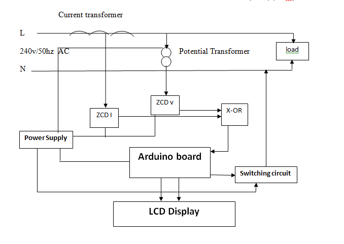
Microcontroller read the RMS value for voltage and current used in its algorithm to select the value of in demand capacitor for the load to correct the power factor and monitors the behaviour of the enduring load on the basis of current depleted by the load. In case of low power factor Microcontroller send out the signal to switching unit that will switch on the in-demand value of capacitor. The tasks executed by the microcontroller for correcting the low power factor by selecting the in demand value of capacitor and load monitoring are shown in LCD.
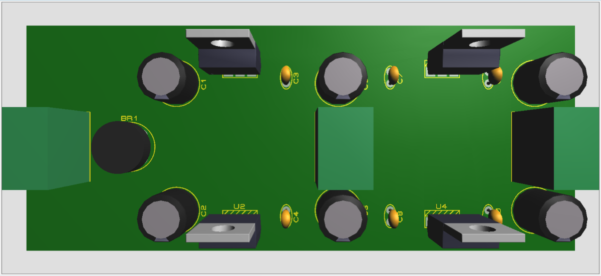
CIRCUIT DIAGRAM:

These two digitized signals i.e. voltage and currents are sent to the microcontroller as the inputs. According to the program written microcontroller calculates the time difference between the zero crossings of these two signals. This time difference is indirectly proportional to the system power factor. The information about this power factor and the power loss is displayed on the LCD display. And according to the range calculated by the microcontroller program; this drives the relays which switches the shunt capacitors across the load.
RESULT:
The expected outcome of this project is to measuring the power factor value displaying it in the LCD and to improve power factor using capacitor bank and reduce current draw by the load using microcontroller and proper algorithm to turn on capacitor automatically, determine and trigger sufficient switching of capacitor in order to compensate excessive reactive components, thus bringing power factor near to unity ,there by improving the efficiency of the system and reducing the electricity bill.
.PNG)
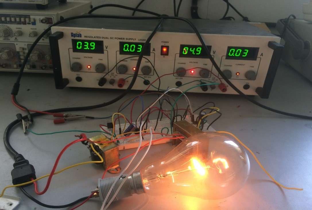
EXPERIMENTAL MODEL:
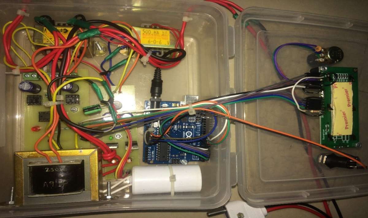
ACTUAL MODEL:
MODEL OUTPUT: