
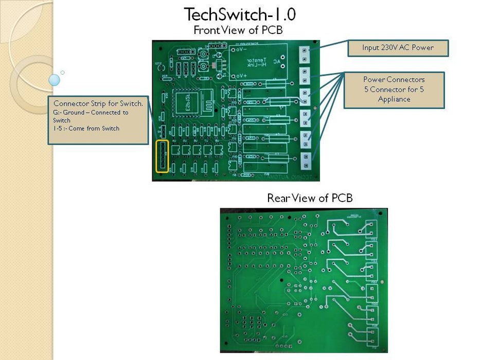
TECHSWTCH 1.0 an OpenSource Smart Switch Hardware (5Cannel)
TECHSWITCH 1.0 PLB Layout

Introduction Video of TechSwitch 1.0
Empower Smart home by TechSwitch-1.0(DIY Mode) .
- What is TechSwitch-1.0(DIY Mode)
- TechSwitch-1.0 is ESP8266 based smart switch. it can control 5 home appliances.
- Why it is DIY mode??
- It is designed to re-flash at any time. there is two mode selection jumper on PCB.
- Run Mode:- for Regular operation.
- Flash Mode :- in this mode user can re-flash chip by following Re-flash procedure.
- Analog Input:- ESP8266 has one ADC 0-1 Vdc. Its header also provided on PCB to play with any Analog sensor.
- It is designed to re-flash at any time. there is two mode selection jumper on PCB.
Technical Specification of TechSwitch-1.0(DIY mode)
- 5 Output(230V AC) + 5 Input(0VDC switching) + 1 Analog input(0-1VDC)
- Rating :- 2.0 Amps.
- Switching element :-- SSR +Zero Crossing switching.
- Protection :- Each output protected by 2 Amp. glass fuse.
- Firmware used:- Tasmota is easy to use and stable firmware. It can be flashed by different firmware as its DIY mode.
- Input :- Opto coupled (-Ve) switching.
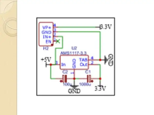
- ESP8266 power regulator can be dual mode:- can use Buck converter as well AMS1117 regulator.
Supplies/Bill Of material
- Power Supply:- Make :- Hi-Link , Model :- HLK-PM01, 230V by 5 VDC, 3W (01)
- Microcontroller:- ESP12F (01)
- 3.3 VDC regulator :- Dual provision any one can be used
- Buck converter (01)
- AMS1117 Voltage regulator.(01)
- PC817 :- Opt coupler Make :- Sharp Package:-THT (10)
- G3MB-202PL:- SSR Make Omron(05), Zero crossing switching.
- LED :-Color:- Any, Package THT (01)
- 220 or 250 Ohm Resistor:- Ceramic (11)
- 100 Ohm Resistor:- Ceramic (5)
- 8k Ohm Resistor :- Ceramic(1)
- 2k2 Ohm Resistor :- Ceramic(1)
- 10K Ohm Resistor:- Ceramic (13)
- Push button :-Part Code:- EVQ22705R, Type:- with Two terminal (02)
- Glass Fuse:- Type :- Glass, Rating :- 2 Amp @ 230V AC. (5)
PCB Male Header:- Three header with Three pin & One header with 4 Pin. so one standard Strip of Male header is preferable to procure.
Designing & Selection of componant Process/Methdology
Step 1: Consept Finalization.

- Finalization of Concept:- I have define requirement as below.
- Making Smart Switch having 5 Switch & Can controlled by WIFI.
- It Can operate withot WIFI by physical Switches or Pushbutton.
- Switch can be DIY mode so it can be RE-Flashed.
- It can fit in existing switch board without changing any switches or wiring.
- ALL GPIO of Microcontroller to be used as it is DIY mode.
- Switching device should SSR & zero crossing to avoide noice & switching surges.
- Size of PCB Should be small enough so it can fit in existing switchboard.
Step 2: Selection of Microcontroller
- As we finalized requirement , next step is to select hardware

- Microcontroller selection criteria.
- Required GPIO :-5 input + 5 Output + 1 ADC.
- Wifi enabled
- Easy to Re-flash to provide DIY functionality.
- Mqtt Support
- HTTP Support
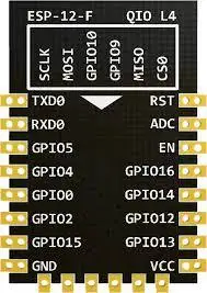
ESP8266 is suitable for above requriement. it has 11 GPIO + 1 ADC + WiFi enabled.
I have selected ESP12F module which is ESP8266 microcontroller based Devlopment board , it has small formfactor & all GPIO are populated for easy use.
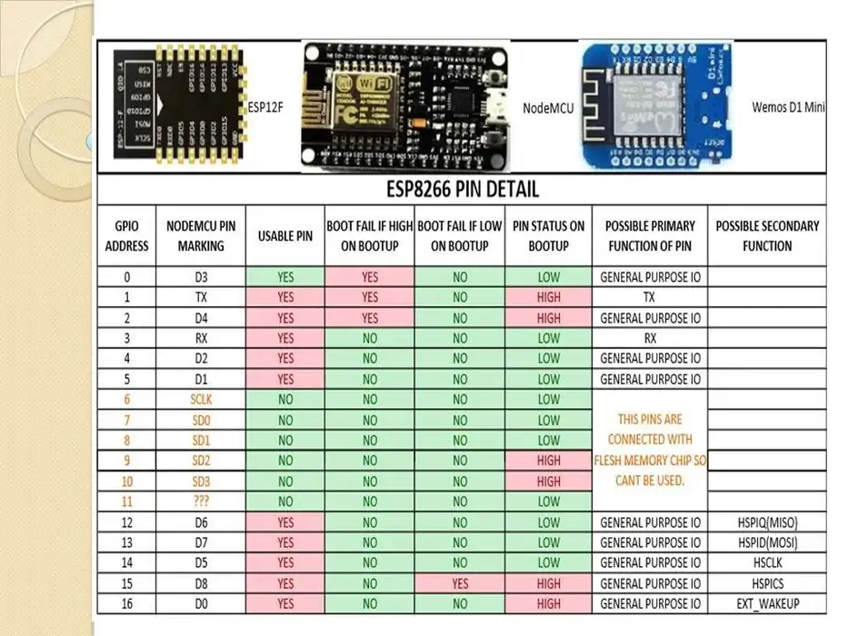
Step 3: Checking GPIO Detail of ESP8266 Board.
Below is GPIO detail of ESP8266 which used to select appropriate GPIO for Input or Output functionality.
- As per ESP8266 Data sheet some GPIO are used for special functions.
- During Breadboard Trial, I scratched my head as not able to boot it plenty of time.
- Finally by research on internet and playing it with breadboard I have summarized GPIO data and made simple table for easy understanding.
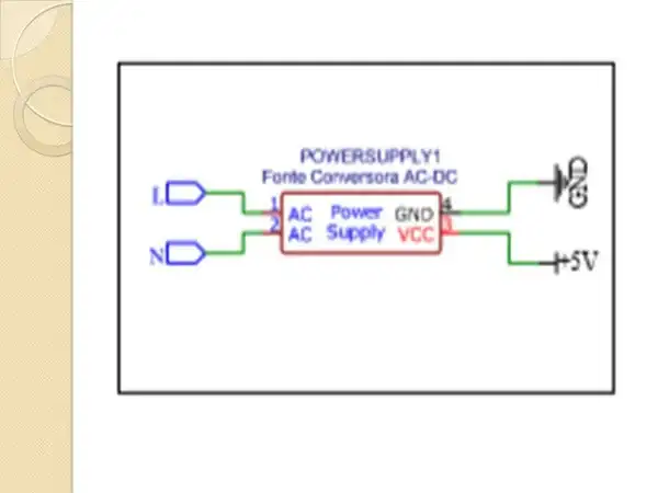
Step 4: Selection of Power Supply.
.webp)
.webp)
- Selection Criteria of Power Supply.
- In India 230VAC is domestic supply. as ESP8266 operates on 3.3VDC, we have to select 230VDC / 3.3VDC power supply.
- Power Switching device which is SSR which operates on 5VDC so i have to select Power Supply having 5VDC as well.
- Finally selected power supply having 230V/5VDC.
- To get 3.3VDC i have selected Buck converter having 5VDC/3.3VDC.
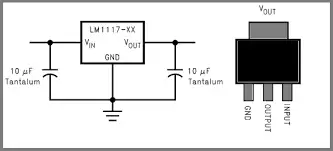
- As we have to design DIY mode i also provide provision of AMS1117 linear voltage regulator.
Final Conclusion.
- First power supply conversion is 230VAC / 5 VDC having 3W capacity.
- HI-LINK make HLK-PM01 smps.
- Second conversion is 5VDC to 3.3VDC
- For this i have selected 5V/3.3V Buck converter.
- i have also kept provision of AMS1117 Linear voltage regulator on PCB so we can use any one which is easily available.
- PCB made in such way it can use AMS1117 or buck converter(Anyone one).
- IF AMS1117 Used then we have to use capacitor for to improve voltage stability.
- Schematic detail is mentioned in schematic explanation section below.
Step 5: Selection of Switching Device.
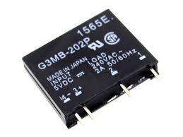
- I have selected Omron Make G3MB-202P SSR
- SSR having 2 amp. current capacity.
- Can operates on 5VDC.
- Provide Zero crossing Switching.
- Inbuilt Snubber circuit.
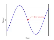
What is Zero Crossing?
- 50 HZ AC supply is sinusoidal voltage.
- Supply voltage polarity changed every 20 mille second & 50 times in one second.
- Voltage gets zero every 20 mille second.
- Zero crossing SSR detects zero potential of voltage and turn on output on at this instance.
- For example :- if command send at 45 Degree (voltage at maximum peak), SSR turned on at 90 degree(when voltage is zero).
- This reduces switching surges & noise.
- Zero crossing point is shown in attached image (Red highlighted text)
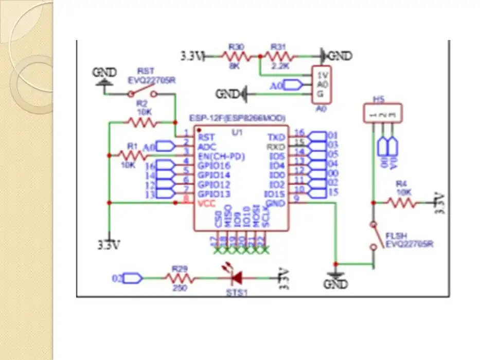
Step 6: ESP8266 PIN Selection.
- ESP8266 has total 11 GPIO and One ADC pin. (Refer Step 3)
- PCB Pin identification
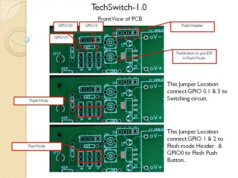
- Pin selection of esp8266 is crucial because of below criteria.
- Criteria for Input selection:-
- GPIO PIN15 Required to be Low during Bootup other wise ESP will not boot.
- It try to bootup from SD card if GPIO15 is High during Bootup.
- ESP8266 neve Boot If GPIO PIN1 or GPIO 2 or GPIO 3 is LOW during bootup.
- GPIO PIN15 Required to be Low during Bootup other wise ESP will not boot.
- Criteria for Output Selection :-
- GPIO PIN 1,2,15 & 16 get High during Bootup(for fraction of time).
- if we use this pin as input & PIN is at LOW level during bootup then this pin gets damaged due to short circuit between PIN which is Low but ESP8266 turin it HIGH during bootup.
- Final conclusion :-
- Finally GPIO 0,1,5,15 & 16 are selected for output.
- GPIO 3,4,12,13 & 14 are selected for Input.
- Criteria for Input selection:-
- Constrain:-
- GPIO1 & 3 is UART pins which are used to flash ESP8266 & we also wanted to use those as output.
- GPIO0 is used to put ESP in flash mode & we also decided to use it as output.
- Solution for above constrain:-
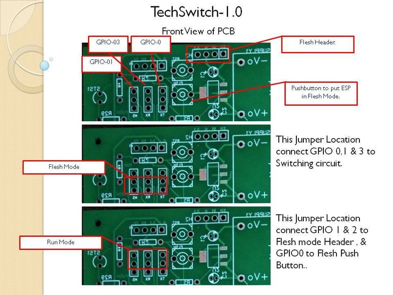
- Problem solved by provide two jumpers.
- Flash mode jumper: - In this position all three pins are isolated from switching circuit and connected to flash mode header.
- Run mode jumper:- In this position all three pins will connected to switching circuit.
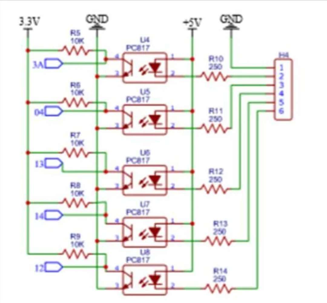
Step 7: Optocoupler Selection.
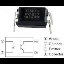
- PIN Detail:-
- PIN 1 & 2 Input Side (Inbuilt LED)
- Pin 1 :- Anode
- Pnd 2 :- Cathode
- PIN 3 & 4 Output Side(Photo transistor.
- Pin 3:- Emitter
- Pin 4 :- Collector
- PIN 1 & 2 Input Side (Inbuilt LED)
- Output switching circuit selection
- ESP 8266 GPIO can feed only 20 m.a. as per esprissif.
- Optocoupler are used to protect ESP GPIO PIN during SSR switching.
- 200 Ohms resistor is used to limit current of GPIO.
- I have used 200, 220 & 250 & all resistors are work fine.
- Current calculation I = V/R, I = 3.3V - 0.7V / 200 Ohms = 13 ma.
.webp)
- Input Switching circuit selection.
- PC817 optocouplers are used in input circuit with 200 ohms current limiting resistor.
- Output of optocoupler are connected with GPIO (defined as Input) along with 10K Pull-up resistor as shown below.
Step 8: Circuit Layout Preparation.
- After selection of all component and define wiring methodology, we can move on to develop Circuit using any pcb designing software.
- i have used Easyeda which is Web based PCB development platform and easy to use.
- URL of Easyeda :- EsasyEda
- For simple explainaiton i have divided whole circuit in chunks. & first is Power circuit.
- Power circuit A:- 230 VAC to 5VDC.
- HI-Link makes HLK-PM01 SMPS used to convert 230Vac to 5 V DC.
- Maximum Power is 3 Watt. means it can supply 600 ma.
- Power circuit A:- 230 VAC to 5VDC.
- Power circuit B:- 5VDC to 3.3VDC.
- As this PCB is DIY mode. i have provide two method to convert 5V to 3.3V.
- Using AMS1117 Voltage regulator.
- Using Buck Converter.
- Anyone can used as per component availability.
Step 9: ESP8266 Wiring
EasyEda used to design schematic of PCB & Net port option is used to make schematic simple.
What is Net port??
- Net post means we can provide name to common junction.
- by using same name in different part, Easyeda will considered all same name as single connected device.
Some basic rule of esp8266 wiring.
- CH_PD pin required to be high.
- Reset pin required to be high during normal operation.
- GPIO 0,1 & 2 shoud not at Low during boot up.
- GPIO 15 should not at High level during Boot up.
- Considering all above points in mind ESP8266 wiring scheme is prepared. & shown in schematic image as mentioned below.
- GPIO2 is used as Status LED & connected LED in Reverse polarity to avoide GPIO2 LOW.
Step 10: ESP8266 Output Switching Circuit
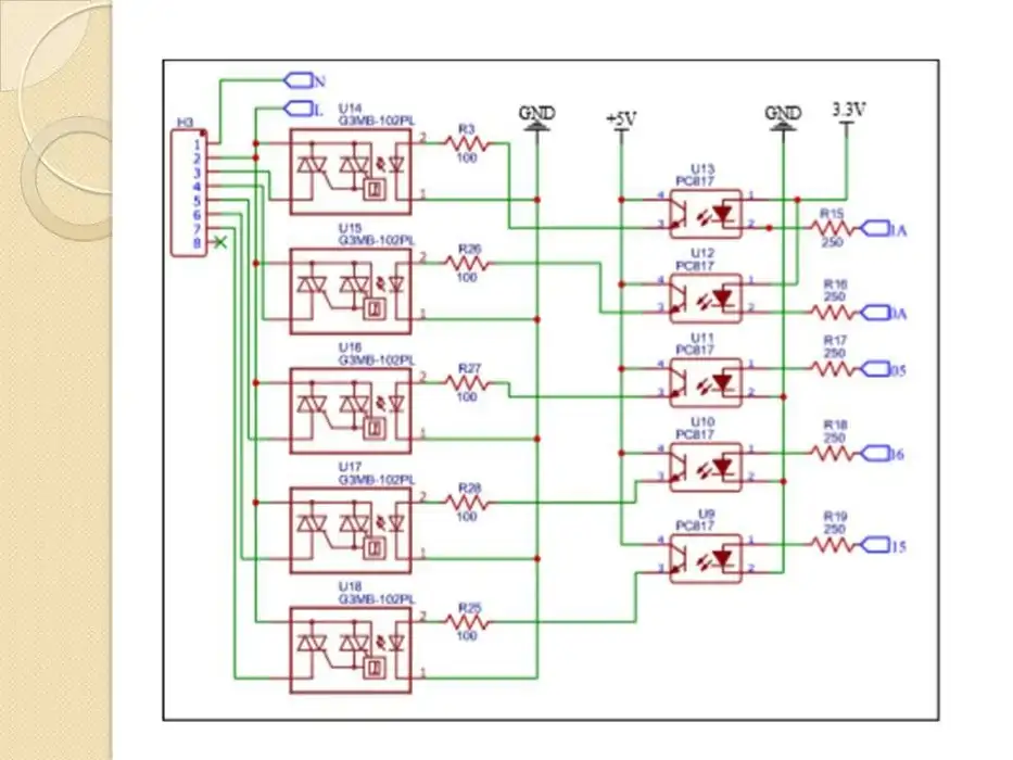
- ESO8266 GPIO 0, 1, 5, 15 & 16 used as output.
- To keep GPIO 0 & 1 at high level its wiring is bit different from other output.
- Booth this pin is at 3.3V during boot up.
- PIN1 of PC817 which is anode is connected to 3.3V.
- PIN2 which is Cathode is connected to GPIO using current limiting resistor(200/220/250 Ohms).
- As forward biased Diode can pass 3.3V(0.7V diode drop) Both GPIO get almost 2.5 VDC during boot up.
- Remaining GPIO pin connected with PIN1 of pc817 which is Anode of PC817 & Ground is connected with PIN2 which is Cathode using current limiting resistor.
- As Ground is connected with Cathode it will pass from PC817 LED and keep GPIO at Low level.
- This makes GPIO15 LOW during boot up.
- We solved problem of all three GPIO by adopting different wiring scheam.
Step 11: Esp8266 Input.
- GPIO 3,4,12,13 & 14 are used as Input.
- As Input wiring will be connected to field device, protection required for ESP8266 GPIO.
- PC817 optocoupler used for input isolation.
- PC817 Input Cathodes are connected with Pin headers using current limiting resistor (250 Ohms).
- Anode of all Optocoupler is connected with 5VDC.
- Whenever Input pin connected to Ground, Optocoupler will get forward biased and output transistor turned on.
- Collector of optocoupler is connected with GPIO along with 10 K Pull-up resistor.
- What is Pull-up???
- Pull-up resistor is used To keep GPIO stable, high value resistor connected with GPIO and another end is connected to 3.3V.
- this keep GPIO at high level and avoid false triggering.
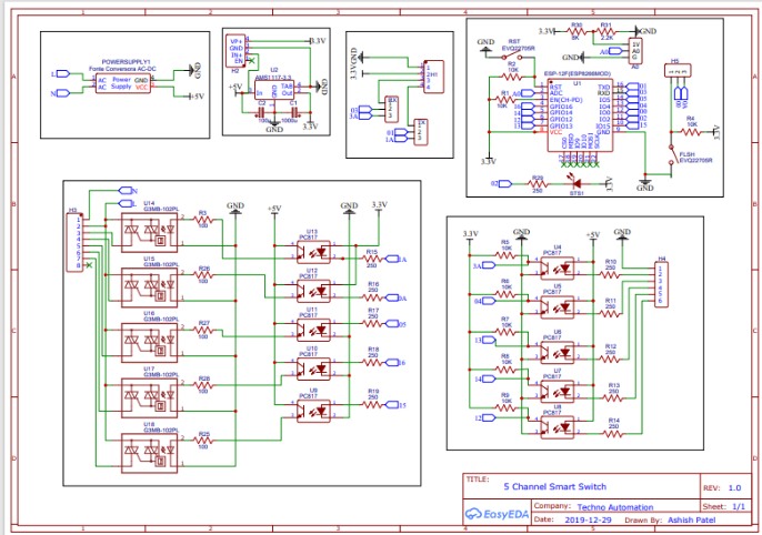
Step 12: Final Schematic
- Final Schematic is as below. After Completion of all parts its time to check wiring.
- Easyeda Provide feature for this.
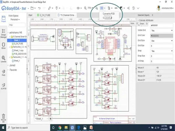
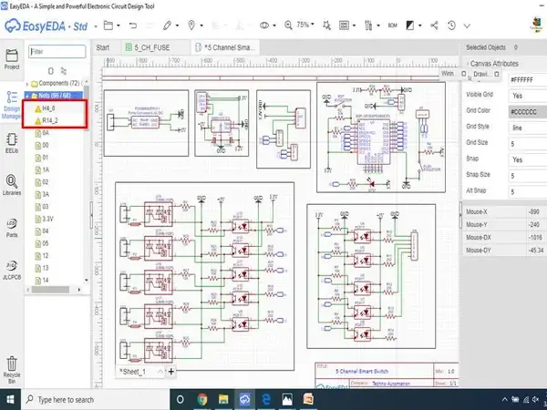
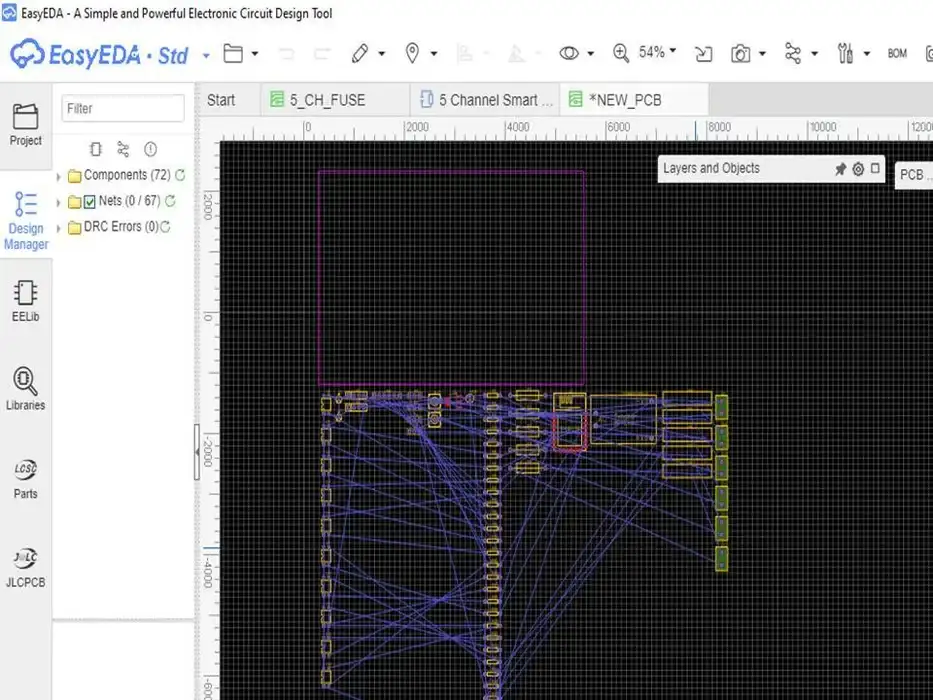
Step 13: Convert PCB
- Steps to convert Circuit in to PCB Layout
- After making Circuit we can convert it in to PCB layout.
- By pressing Convert to PCB option of Easyeda system will start conversion of Schematic in to PCB Layout.
- If any wiring error or unused pins are present then Error/Alarm generates.
- By checking Error in Right side section of Software development page we can resolve each error one by one.
- PCB layout generated after all error resolution.
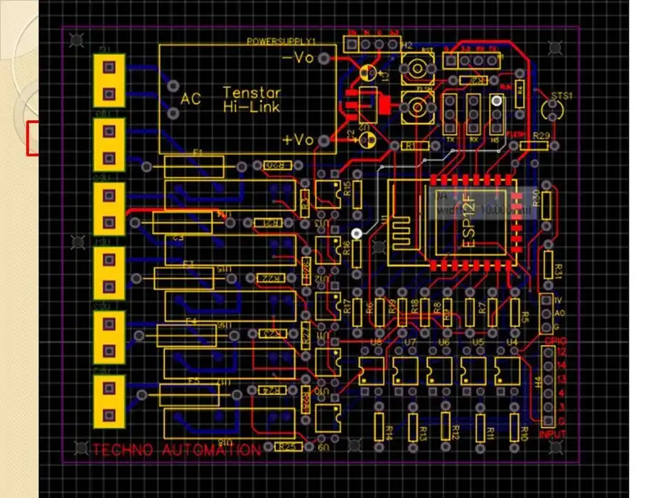
Step 14: PCB Layout & Componant Arrangement.
- Componant Placement
- All components with its actual
- dimensions and labels are shown in PCB layout screen.
- First step is to arrange component.
- Try to put High voltage and Low voltage component as far as possible.
- Adjust each component as per required size of PCB.
- After arranging all components we can make traces.
- (traces width required to be adjust as per current of circuit part)
- Some of traces are traced in bottom of pcb using layout change function.
- Power traces are keeping exposed for soldering pouring after fabrication.
Step 15: Final PCB Layout.
- Finaliized all componant layout as shown below.
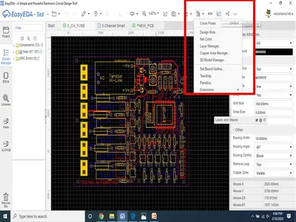
Step 16: Checking 3D View and Generating Ggerber File.
- Easyeda provide 3D view option in which we can check 3D view of PCB and get idea how it looks after fabrication.
.webp)
- After checking 3D view Generate Gerber files.
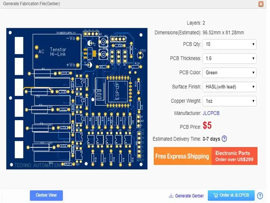
Step 17: Placing Order.
- After Generation of Gerber file system provides Front view of final PCB layout and cost of 10 PCB.
- We can place order to JLCPCB directly by pressing "Order at JLCPCB" Button.
- We can select color masking as per requirement and select mode of delivery.
- By placing order and making payment we get PCB within 15-20 days.
Step 18: Recieving PCB.
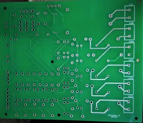
- Visually inspect PCB front and back after receiving it which looks good.
- Front side of PCB
.webp)
- Back Side of PCB
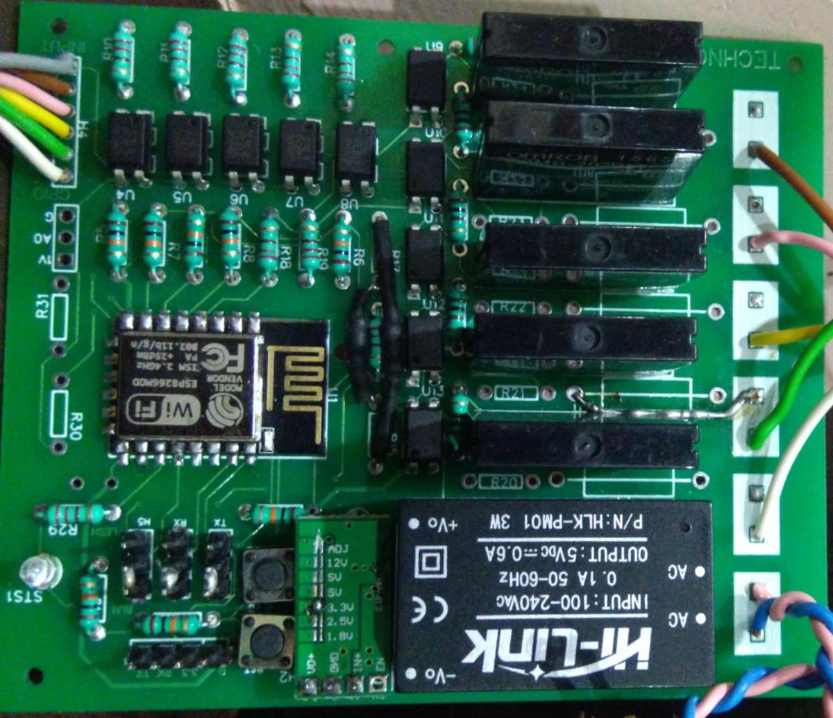
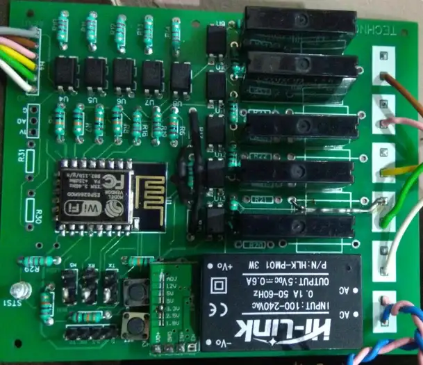
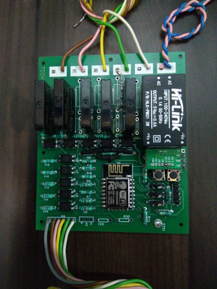
Step 19: Componant Soldring on PCB.
- As per component identification ON PCB all components soldering started.
- Take Care:- Some part footprint is backward side so check labeling on PCB and part manual before final soldering.
- Front View after soldring all componants
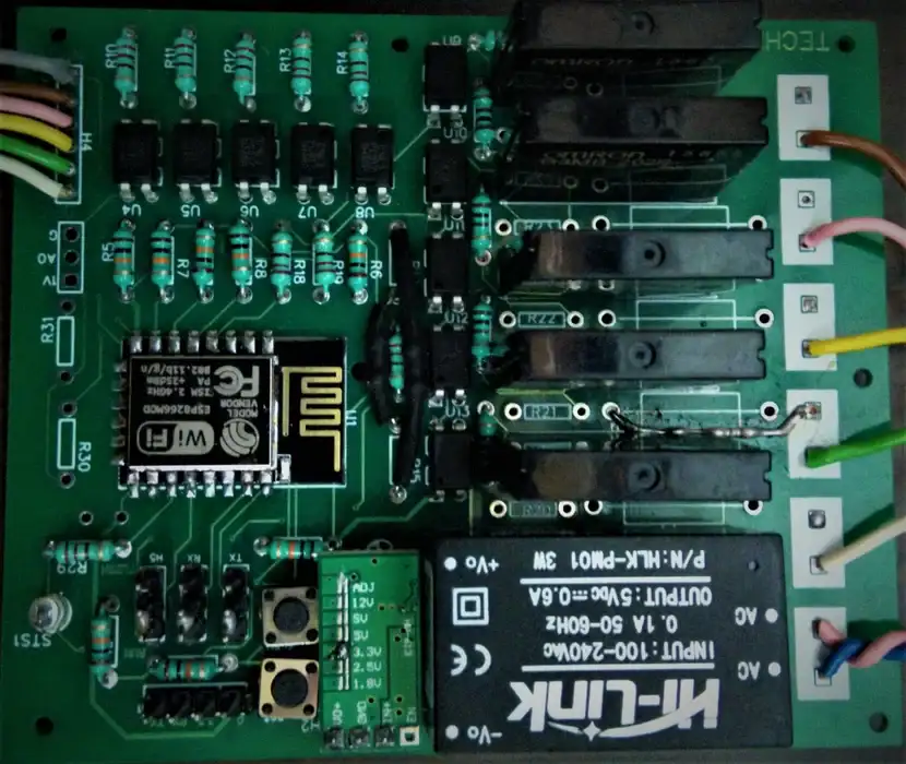
Step 20: Power Track Thickness Increasing.
- For power connection tracks I put open tracks during PCB layout process.
- As shown in image all power traces are open so poured extra soldering on it to increase currant caring capacity.
.webp)
Step 21: Final Checking
- After soldering of all components cheked all components using multimeter.
- Resistor value checking
- Optocoupler LED checking
- Grounding checking.
Step 22: Flashing Firmware.
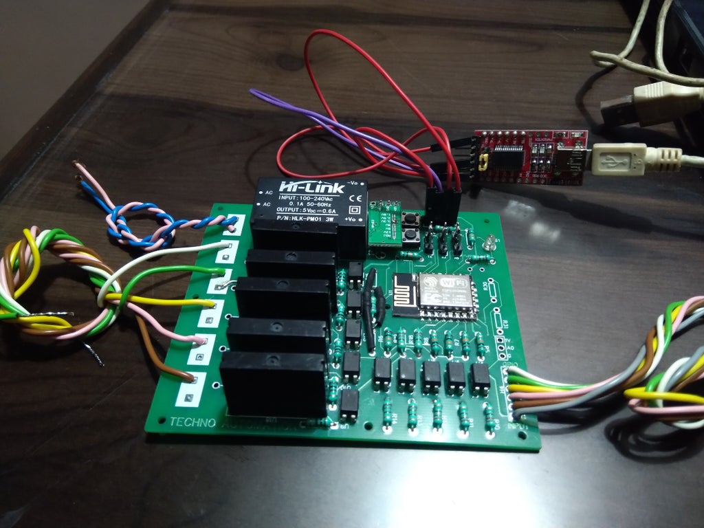
- Three jumpers of PCB are used to put esp in boot mode. Jumper identificatino is as below.
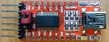
- Check Power selection Jumper on 3.3VDC of FTDI Chip.
- Connect FTDI chip to PCB
- Wiring of FTDI to PCB as below.
- FTDI TX :- PCB RX
- FTDI RX :- PCB TX
- FTDI VCC :- PCB 3.3V
- FTDI G :- PCB G
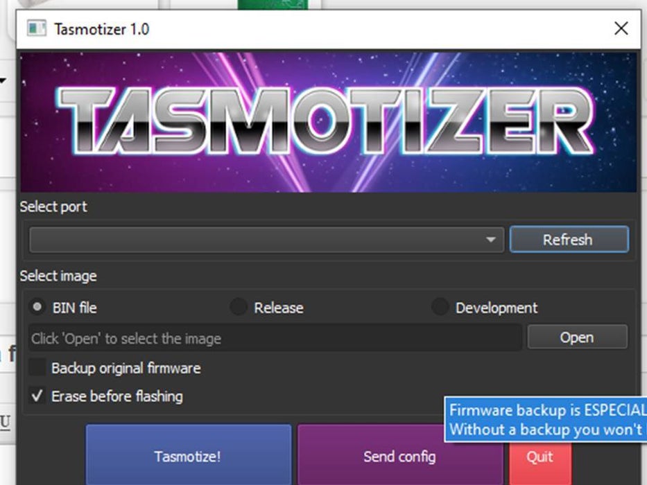
Step 23: Flash Tasamota Firmware on ESP8266
- Steps for Tasmota fleshing is as below.
- Download Tasamotizer which is fleshing tool for esp8266 board
- Download tasmota firmware pre compiled bin file known as:- Tasmota.bin
- Install tasmotazer and open it.
- In tasmotizer click select port drill dawn button.
- if FTDI is connected then port appear in list.
- Select port from list.(in case multiple port, check which port is of FTDI)
- click open button and Select Tasamota.bin file from download location.
- click on Erase before flashing option(clear spiff if any data is there)
- Press Tasamotize! Button
- if everything is ok then you get progressbar of erasing flash.
- once process completed it shows "restart esp" popup.
Step 24: Seting Tasmota
- Tasmota configration online help:-Tasmota configration help
- Connect AC power to PCB
- ESP will start and Status led of PCB flash once. Open Wifimanger on Laptop and search for new AP named start with "Tasmota"
- Connect Tasmota Network which didnt ask for password. once connected webpage opened automatically.
- If Webpage not opened then open Webpage and enter 192.168.4.1 and hit enter will pen tasmot configuration page.
- Configure WIFI ssid & Password of your router in Configure Wifi page( Two Wifi Ap can also saved by Tasmota).
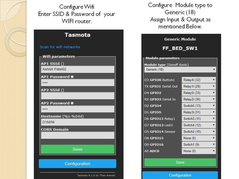
- Device will restart after saving.
- Open your router, check for new device ip & note its IP.
- open webpage and enter that newly connected IP in Webpage to start device setting.
- Set Module type(18) in configure module option and set all input & output as mentioned in configuration image shown above.
- restart PCB and its good to go.
Step 25: Wiring Guide and Demo
- Final Wiring & Trial of PCB
- Wiring of all 5 inputs are connected to 5 Switch/Buttone.
- Second connection of all 5 device is connected to Common "G" wire of input header.
- Output side 5 Wire connecton to 5 home appliance.
- Give 230 to input of PCB.
- Smart Swith with 5 Input & 5 Output is ready to use.
Demo of trial :- Demo on Youtube is hear.
Step 26: To DO list for future.
- Power connection track thinking.
- PCB size optimization.
- Adding 6th SSR with GPIO2 which can controlled by Analogue input.