1. Project Overview and Concept
The Multifunctional IC Tester is an integrated diagnostic instrument designed to replace bulky laboratory equipment with a single, portable, ESP32-powered device. It bridges the gap between a standard Digital Multimeter (DMM) and a logic analyzer by offering high-precision analog measurements alongside automated digital and linear IC verification.
2. Hardware Architecture & Component Selection
The core of the system is the ESP32 DevKit V1, selected for its high-resolution 12-bit ADC (Analog-to-Digital Converter) and dual-core processing capabilities, which allow for simultaneous signal processing and UI management.
Key Hardware Blocks:
- Measurement Interface: A series of voltage dividers and current sensors (ACS712) for analog parameters.
- Auto-Ranging Unit: A transistor-switched resistor network using BC547 NPN transistors to dynamically adjust the measurement range.
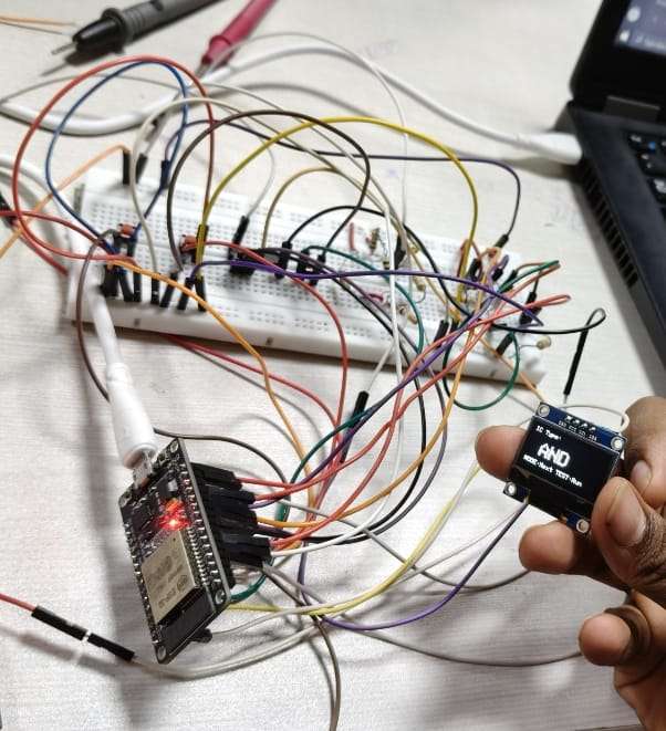
- Testing Socket: A 14-pin ZIF (Zero Insertion Force) socket for non-destructive testing of various IC families.
- User Interface: A 0.96" I2C OLED display and tactile buttons for mode selection and result visualization.
3. Step-by-Step Functional Modules
Step 1: High-Voltage DC Measurement
Standard microcontrollers cannot read voltages above 3.3V. We implemented a calibrated voltage divider ($33\text{k}\Omega$ and $3\text{k}\Omega$) to scale external DC sources (up to 35V) down to a safe ADC range. The firmware applies a correction factor to account for resistor tolerances, achieving a measured accuracy of 99.2%.
Step 2: Intelligent Auto-Ranging Ohmmeter
This is the most technically advanced part of the DMM module. Instead of a fixed reference, the device utilizes three reference resistors ($1\text{k}\Omega$, $10\text{k}\Omega$, $100\text{k}\Omega$).
- The ESP32 takes a "pre-scan" reading using the $10\text{k}\Omega$ resistor.
- If the result is outside the optimal linear range of the ADC, it triggers a transistor to switch to a higher or lower reference resistor.
- The final calculation is performed using the updated reference, ensuring 98.5% accuracy across a wide range of resistances.
Step 3: Capacitance and Continuity
- Capacitance: The system measures the RC Time Constant. It charges the unknown capacitor through a precision resistor and times how long it takes to reach 63.2% of the source voltage.
- Continuity: A low-latency digital loop checks for a direct path between probes, providing instant visual feedback on the OLED.
Step 4: Digital IC Logic Verification
The device tests 74-series logic gates (AND, OR, NAND, XOR, etc.) using a automated truth-table validation algorithm:
- The user selects the IC type from the menu.
- The ESP32 sets the respective GPIOs as outputs (for IC inputs) and inputs (for IC outputs).
- It cycles through all possible binary input combinations (e.g., 00, 01, 10, 11 for a 2-input gate).
- The measured outputs are compared against a hardcoded truth-table. If even one bit fails, the device flags the IC as faulty.
Step 5: Linear IC Testing (Op-Amps)
For linear components like the LM741, the device configures a basic circuit (typically a voltage follower or inverting amplifier). It applies a known DC voltage and reads the output via the ADC. If the output matches the theoretical gain equation within a ±10% tolerance, the IC is passed as functional.
4. Software Design and UI Logic
The firmware is written in C++ using the Arduino framework. It employs a State Machine architecture, ensuring that the device is only in one mode at a time to prevent pin conflicts.
- Interrupt Handling: Push buttons use debouncing logic to ensure clean mode transitions.
- Averaging Algorithm: To overcome the ESP32’s ADC noise, every measurement is the result of 64 samples averaged together, providing the stable readings seen in the final results.
5. Conclusion and Results
The project successfully achieves the goal of a low-cost, portable diagnostic tool. With a build cost of approximately 300-500 INR, it offers functionality that would typically cost over 3,000 INR in commercial markets. The device is not just a tool but a platform for future expansion, including wireless data logging and automatic IC identification.