





This project presents a Secure Digital Access Control System built using a Finite State Machine (FSM) on the DE1-SoC FPGA board. The system allows users to enter a 4-digit password through a keypad or switches, verifies the password in hardware, and provides feedback through LEDs, 7-segment displays, a TFT screen, and a buzzer. To improve security, the system includes an inactivity timeout and a 15-second lockout mechanism after three failed attempts. The complete hardware is assembled inside a custom 3D-printed enclosure, making it a practical FPGA-based prototype for access control applications.
1 DE1-SoC FPGA Board Overview
The DE1-SoC FPGA Board is a powerful embedded development system platform that is developed to support embedded applications and digital system design. It is designed based on the Altera System-on-Chip (SoC) FPGA that combines a dual-core ARM Cortex-A9processor with programmable logic on a single chip. This integration enables designers to integrate hardware as well as software capabilities in a single system with high flexibility and performance. The board uses a 12V power adapter and communicates with a computer via a USB Type-A to Type-B cable allowing it to be easily programmed and debugged via the onboard USB-Blaster II interface in JTAG mode. Figure 1 shows the DE1-SoC FPGA board.

Figure 1: DE1-SoC FPGA Board
Regarding physical layout, the board has a large variety of onboard components, as depicted in Figure 2 (top view) and Figure 3 (bottom view). These models depict the position of connectors, interfaces, and other important hardware components that facilitate the development of the system. The board is divided into two major sections, the FPGA (programmable logic) part and the Hard Processor System (HPS) part, which offer various functions to implement the system
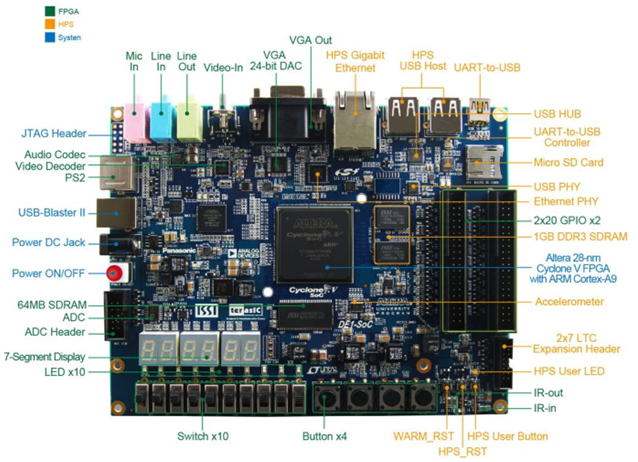
Figure 2: DE1-SoC Development Board (Top View)
.png)
Figure 3: DE1-SoC Development Board (Bottom View)
The FPGA section relies on the Altera Cyclone5CSEMA5F31C6N device and features a few critical hardware features which assist in the design and testing of digital designs:
- USB-Blaster II for FPGA configuration using JTAG mode
- 64MB SDRAM with a 16-bit data bus
- Four pushbuttons and ten slide switches for user input
- Ten red user LEDs and six 7-segment displays for output indication
- Four 50 MHz clock sources from the onboard clock generator
- Two 40-pin GPIO expansion headers with diode protection circuitry
- An A/D converter with a 4-pin SPI interface
Moreover, embedded processing is offered in the HPS section by utilizing the ARM-based processor and the peripherals:
- 800 MHz dual-core ARM Cortex-A9 MPCore processor
- 1GB DDR3 SDRAM with a 32-bit data bus
- Gigabit Ethernet interface with RJ45 connector
- Two USB host ports (Type-A)
- Micro SD card slot for storage
- Accelerometer with I2C interface and interrupt support
- UART-to-USB interface using a USB Mini-B connector
- Warm reset and cold reset buttons
- One user button and one user LED
- LTC 2×7 expansion header
The DE1-SoC board is a full and highly integrated hardware platform that is useful in both logic design and embedded system development on an FPGA. Its ability to have extensive onboard peripherals, input/output interfaces and expandability make it very appropriate in the implementation of complex systems like the FSM-based secure digital access control system that was created in this project.
2 Block Diagram of the DE1-SoC Board
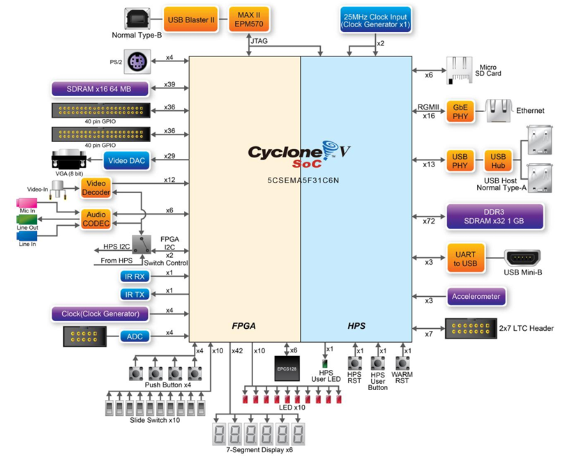
Figure 4: Block Diagram of DE1-SoC
The block diagram of the DE1-SoC FPGA Board is given in Figure 4, which depicts the connection between all the parts of the system with each other through the core Cyclone V SoC FPGA core. It is highly flexible architecture, with the FPGA being programmable to allow users to build their own digital systems as well as making use of the embedded processor to carry out more complex control and processing endeavours. In general, the block diagram shows a highly integrated system in which all the elements are linked to each other via the Cyclone V SoC.
3 GPIO Expansion Header Overview
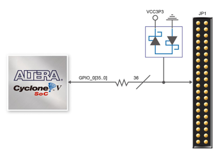
Figure 5: Connections between the GPIO header and Cyclone V SoC FPGA
The DE1-SoC FPGA Board provides two 40-pin GPIO expansion headers for connecting external peripherals, as shown in Figure 5. Each header includes 36 customizable I/O pins connected to the Cyclone V SoC FPGA.
The headers also provide +5V, +3.3V, and GND pins, which can power external modules such as displays, keypads, and sensors. However, the current limits must be followed: 1A maximum for 5V and 1.5A maximum for 3.3V.
The GPIO pins include protection using series resistors and clamping diodes. These protect the FPGA from voltage spikes, negative voltage, and incorrect signal levels. Therefore, the GPIO headers allow safe connection to external devices, provided that proper voltage and current limits are maintained.
Table 1: Voltage and Max. Current Limit of Expansion Header(s)
| Supplied Voltage | Max. Current Limit |
| 5V | 1A |
| 3.3V | 1.5A |
In general, the GPIO expansion headers provide flexibility and protection to the FPGA as the primary interface with the peripherals.
4 Methodology
4.1 Block Diagram of the Overall Hardware Architecture
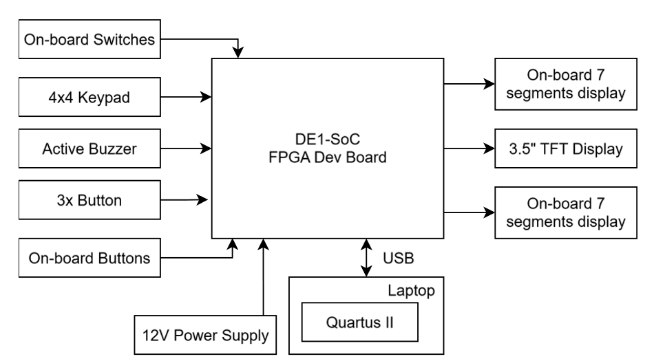
Figure 6: Block Diagram of the Overall Hardware Architecture
Figure 6 presents the overall hardware architecture of the Secure Digital Access Control System. At the center is the DE1-SoC FPGA Board, which acts as the main processing unit. It handles all inputs, executes the FSM-based control logic, and generates the corresponding outputs.
On the input side, the system includes a 4×4 keypad, onboard switches, onboard pushbuttons, and three external buttons. The keypad and switches are mainly used for entering password digits, while the buttons handle control actions such as confirmation, clearing inputs, and system reset.
On the output side, the FPGA controls multiple devices. The onboard 7-segment displays show the entered password for immediate visual feedback. A 3.5-inch TFT display provides more detailed system information, such as status messages. Additionally, an active buzzer delivers audio alerts, especially for incorrect passwords or system lockout.
The system is powered by a 12V power supply to ensure stable operation. A laptop running Quartus II connects to the FPGA via USB for programming, uploading the Verilog design, and performing debugging or testing.
4.2 Schematic Diagram of External Peripherals
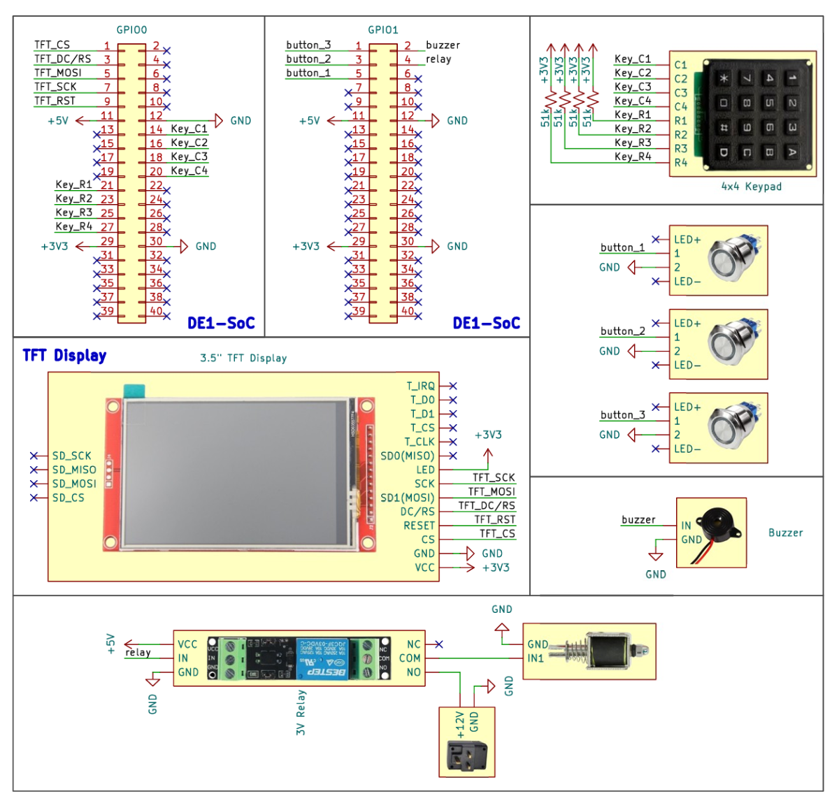
Figure 7: Schematic Diagram of External Peripherals
Figure 7 shows the schematic diagram of the external peripherals connected to the DE1-SoC FPGA Board through GPIO0 and GPIO1 headers.
GPIO0 is mainly used for user input and display. The 3.5-inch TFT display is connected using SPI signals, including chip select, data/command, MOSI, clock, backlight, and reset. This allows the FPGA to display password input, access status, and error messages. The 4×4 keypad is also connected to GPIO0 using four row lines and four column lines, allowing the FPGA to detect key presses through keypad scanning.
GPIO1 is used for control buttons and audio feedback. Three external push buttons are connected to GPIO1 for functions such as reset, confirmation, and special control actions. An active buzzer is also connected to GPIO1, allowing the FPGA to produce sound alerts for events such as wrong password entry or system lockout.
4.3 Schematic Diagram of On-Board Peripherals and Displays
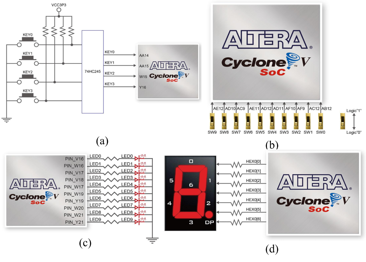
Figure 8: Schematic Diagram of On-Board Peripherals and Displays (a) Pushbuttons (b) Slide Switches (c) LEDs (d) 7-Segment Displays
Figure 8 shows the schematic diagram of the onboard peripherals and displays used in the system.
The onboard pushbuttons KEY0, KEY1, and KEY2 are used for confirm, clear, and full system reset functions. These buttons are active-low and include hardware debouncing through the board circuit, which helps provide stable input signals.
The onboard slide switches SW0 to SW9 are used as an alternative method for entering digits 0 to 9. This is useful for testing and debugging the password input without relying only on the external keypad.
Five onboard LEDs are used to show the system status and wrong password attempts. LED0 indicates idle or locked status, LED1 indicates successful access, and LED2 to LED4 show the number of incorrect attempts. After the third wrong attempt, the buzzer is also activated.
The onboard 7-segment displays HEX0 to HEX3 show the entered 4-digit password in real time. HEX3 displays the first digit, while HEX0 displays the last digit. Since the displays are common-anode, logic 0 turns a segment ON.
Overall, the onboard peripherals provide alternative input, visual feedback, and testing support, making the FSM-based access control system easier to operate and debug.
4.4 3D Enclosure Design of the Secure Digital Access Control System
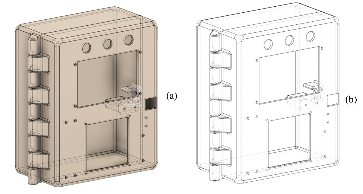
Figure 9: 3D Enclosure Design of the Secure Digital Access Control System
Figure 9 shows the 3D enclosure design of the Secure Digital Access Control System. The enclosure was designed in Autodesk Fusion to provide a compact and organized housing for the system components.
The enclosure size is 160.88 mm × 178 mm × 85.8 mm, allowing enough space for the DE1-SoC FPGA Board and external peripherals. It is divided into a front section and a back section.
The front section holds the user interface components, including the TFT display, keypad, and three external buttons. The back section is used to securely fit the FPGA board. Overall, the enclosure keeps the hardware stable, compact, and easy to operate.
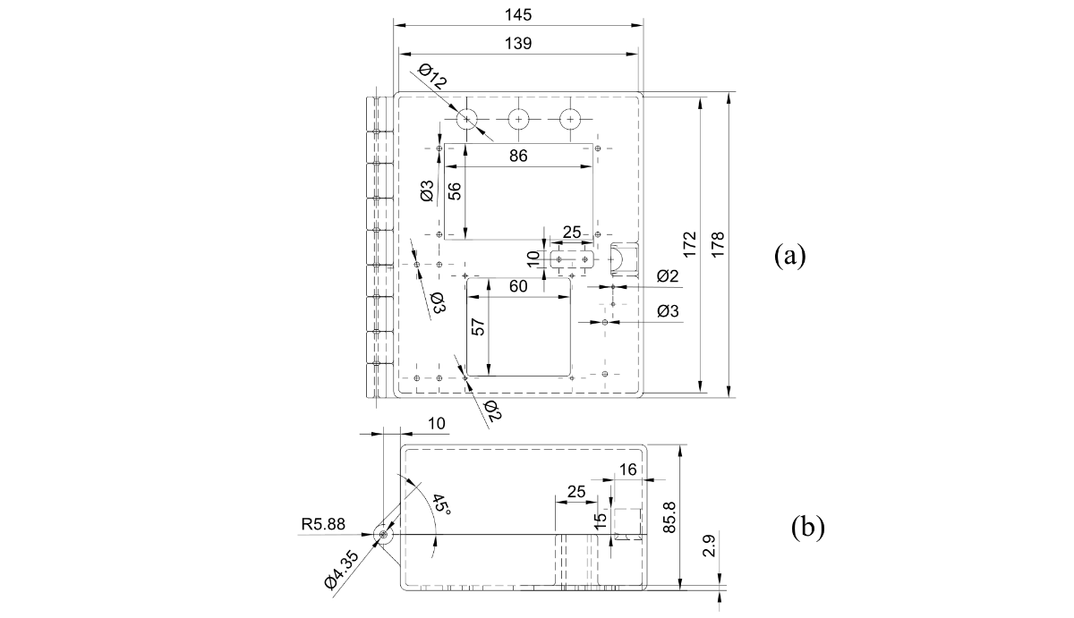
Figure 10: Dimension Drawing of the 3D Enclosure Design (a) Front View (b) Top View
Figure 10 shows the enclosure dimension drawing, while Figure 11 shows the component layout of the 3D enclosure.
The enclosure includes a 1.75 mm filament hinge, allowing the front and back sections to open and close easily without using extra mechanical hinges. This makes the design simpler and easier to assemble.
The front panel includes three circular holes for the external buttons, a large rectangular opening for the TFT display, and another cutout below it for the keypad. These placements make the input and output components easy to access.
A side opening is also added for the lock opener mechanism. This allows the solenoid lock to be manually activated during debugging or troubleshooting, making it easier to access the internal wiring safely.
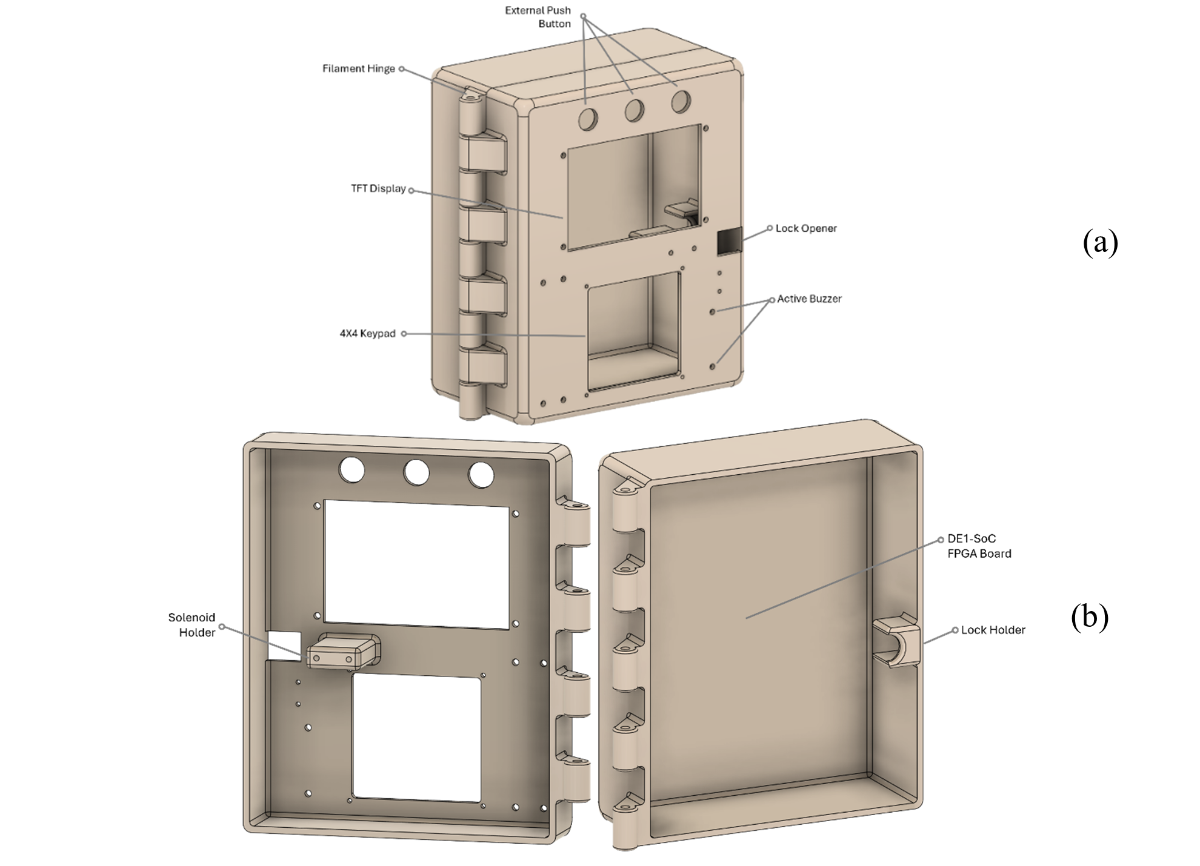
Figure 11: 3D Enclosure Design (a) External View (b) Internal View
4.5 3D Printing
The enclosure was fabricated using FDM 3D printing, providing a low-cost and efficient method for producing a customized hardware case.
It was printed using Cherry Blossom Pink PETG filament due to its durability, slight flexibility, and better heat resistance compared to PLA. The enclosure was printed in two main parts: the top section weighing about 95 g and the bottom section weighing about 143 g.
A fuzzy skin texture was applied to the outer surface to reduce visible layer lines and give the enclosure a cleaner, more finished appearance.
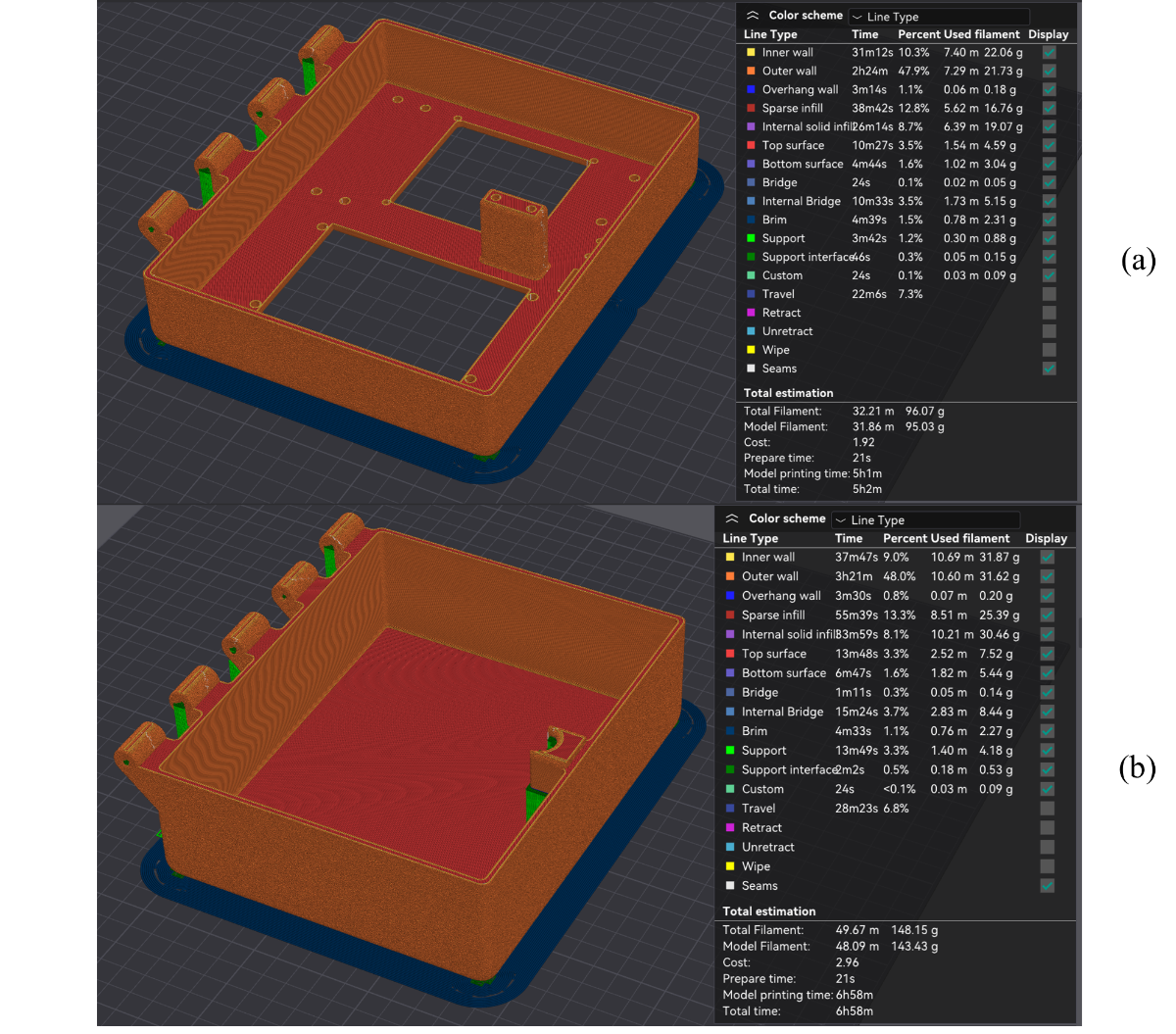
Figure 12: 3D Printing Process of Enclosure (a) Top Part (b) Bottom Part
4.6 Assembled Hardware Integration in Enclosure
Figure 13 shows the assembled hardware. The completed hardware can then be used to assemble all the designed components in a small functional enclosure to create a complete Secure Digital Access Control System. The enclosure consists of two primary parts, the right side contains the DE1-SoC FPGA board, and the left side contains the support circuitry, the breadboard, solenoid lock mechanism and active buzzer. The FPGA board is firmly fixed to allow stability, and the GPIO0 and GPIO1 headers are linked using ribbon cables to allow the connection of the external hardware, 4x4 keypad, TFT display and external pushbuttons.
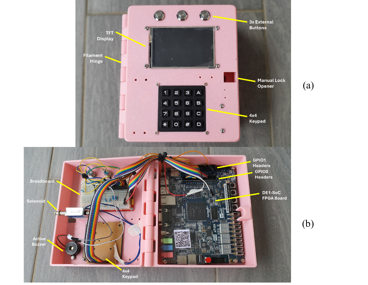
Figure 13: Assembled hardware of the Secure Digital Access Control System inside the enclosure (a) External Views (b) Internal Views
In general, the complete system is a well-structured and realistic implementation of hardware. The system is lightweight, and its total weight is about 700g.
4.7 Overall System Flowchart
.png)
.png)
Figure 14: Simplified System Flowchart of the Secure Digital Access Control System
The general system flow diagram shows the operation of the Secure Digital Access Control System from power-up to final output.
After power-up, the system initializes for about 1.3 ms to ensure all hardware signals are stable. It then enters the ready state and waits for user input. If the reset button is pressed, the system restarts the process.
The system continuously checks inputs from the 4×4 keypad, slide switches, and push buttons. The keypad is scanned using row and column signals, while the switches provide an alternative digit input method. The push buttons are used for submit, clear, and reset functions.
Entered digits are stored in order until four digits are received. If the clear button is pressed, all stored digits are removed. When submit is pressed, the system verifies the password. A correct password grants access, while an incorrect password increases the failed attempt counter. After three wrong attempts, the system enters a 15-second lockout state.
An idle timer is also included. If no input is detected for about 10 seconds, the entered digits are automatically cleared to prevent unfinished inputs from remaining in the system.
The FSM controls the whole process using seven states: IDLE, ENTRY, VERIFY, GRANTED, DENIED, LOCKOUT, and TIMEOUT. Based on user input and system conditions, the FSM moves between these states and returns to IDLE after each operation.
The system outputs feedback through the buzzer, LEDs, 7-segment displays, and TFT screen. These outputs show access status, wrong attempts, timeout, lockout, and the digits entered by the user.
4.8 State Table
The Secure Digital Access Control System has a control subsystem, which is implemented based on a MooreFinite State Machine (FSM) architecture. The outputs in a Moore machine are only influenced by the existing state and not the input signals, which enhances better stability in a system and eliminates glitches during input transitions.
Table 2: State Encoding of the Moore FSM implementation
| State Label | State Name | One-Hot | Binary |
| S0 | IDLE | 0000001 | 000 |
| S1 | ENTRY | 0000010 | 001 |
| S2 | VERIFY | 0000100 | 010 |
| S3 | GRANTED | 0001000 | 011 |
| S4 | DENIED | 0010000 | 100 |
| S5 | LOCKOUT | 0100000 | 101 |
| S6 | TIMEOUT | 1000000 | 110 |
Table 3: State Transition Table of the Moore FSM implementation
| Current State | Condition | Next State |
| S0 (IDLE) | key_valid | S1 (ENTRY) |
| S0 (IDLE) | submit_request | S2 (VERIFY) |
| S0 (IDLE) | clear_request | S1 (ENTRY) |
| S0 (IDLE) | inactivity_timeout | S6 (TIMEOUT) |
| S0 (IDLE) | none | S0 (IDLE) |
| S1 (ENTRY) | submit_request | S2 (VERIFY) |
| S1 (ENTRY) | clear_request | S0 (IDLE) |
| S1 (ENTRY) | inactivity_timeout | S6 (TIMEOUT) |
| S1 (ENTRY) | none | S1 (ENTRY) |
| S2 (VERIFY) | password_ok | S3 (GRANTED) |
| S2 (VERIFY) | password_fail | S4 (DENIED) |
| S3 (GRANTED) | always | S0 (IDLE) |
| S4 (DENIED) | always | S0 (IDLE) |
| S5 (LOCKOUT) | !lockout_active | S0 (IDLE) |
| S5 (LOCKOUT) | lockout_active | S5 (LOCKOUT) |
| S6 (TIMEOUT) | always | S0 (IDLE) |
| any | lockout_active | S5 (LOCKOUT) |
Table 4: Output Table of the Moore FSM showing state-dependent output signals
| State | grant_pulse | deny_pulse | timeout_pulse |
| S0 (IDLE) | 0 | 0 | 0 |
| S1 (ENTRY) | 0 | 0 | 0 |
| S2 (VERIFY) | 0 | 0 | 0 |
| S3 (GRANTED) | 1 | 0 | 0 |
| S4 (DENIED) | 0 | 1 | 0 |
| S5 (LOCKOUT) | 0 | 0 | 0 |
| S6 (TIMEOUT) | 0 | 0 | 1 |
4.9 State Diagram
FSM has seven states (S0, S1, S2, S3, S4, S5, S6): IDLE (S0), ENTRY (S1), VERIFY (S2), GRANTED (S3), DENIED (S4), LOCKOUT (S5), and TIMEOUT (S6). Every state is a distinct phase of system work, waiting until a user activates the system, authentication findings, and security measures. The system starts at the IDLE state and switches between states depending on conditioned input signals like key_valid, submit request, clear request and inactivity-timeout which guarantee structured and controlled system behaviour.
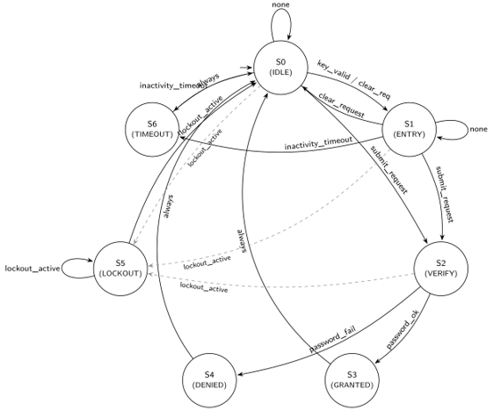
Figure 15: Moore FSM state diagram of the secure digital access control system showing all states and transitions.
The FSM states are represented using one-hot encoding for FPGA implementation. This method is chosen because it simplifies combinational logic and improves timing performance.
The state transition table defines how the system moves between states based on input conditions. For example, the system only enters VERIFY after the submit button is pressed, enters LOCKOUT after three failed attempts, and enters TIMEOUT when inactivity is detected. These transitions help prevent invalid states, deadlocks, and unintended loops.
The output table follows the Moore machine concept, where outputs depend only on the current state. For example, the GRANTED state activates the unlock signal, while the DENIED and TIMEOUT states generate feedback signals.
Overall, the FSM provides secure password checking, lockout after three wrong attempts, and inactivity timeout. It works together with the input conditioning, datapath, and output control modules to ensure stable and coordinated system operation.
5 Results & Discussions
5.1 Hardware Testing Results and Discussion
The DE1-SoC FPGA board was used to test the real-time operation of the Secure Digital Access Control System and verify the implemented Verilog design.
During testing, LEDR0 indicates the locked state, while LEDR1 indicates successful access. The system accepts password input from both onboard slide switches and the external 4×4 keypad. The entered digits are displayed on the 7-segment displays and also shown on the TFT screen, allowing users to check their input clearly.
As Figure 16 (b) illustrates, when switch ON SW5, the 7-segment display effectually displays digit 5, and when pressing a key on the keypad, the same digit is displayed.
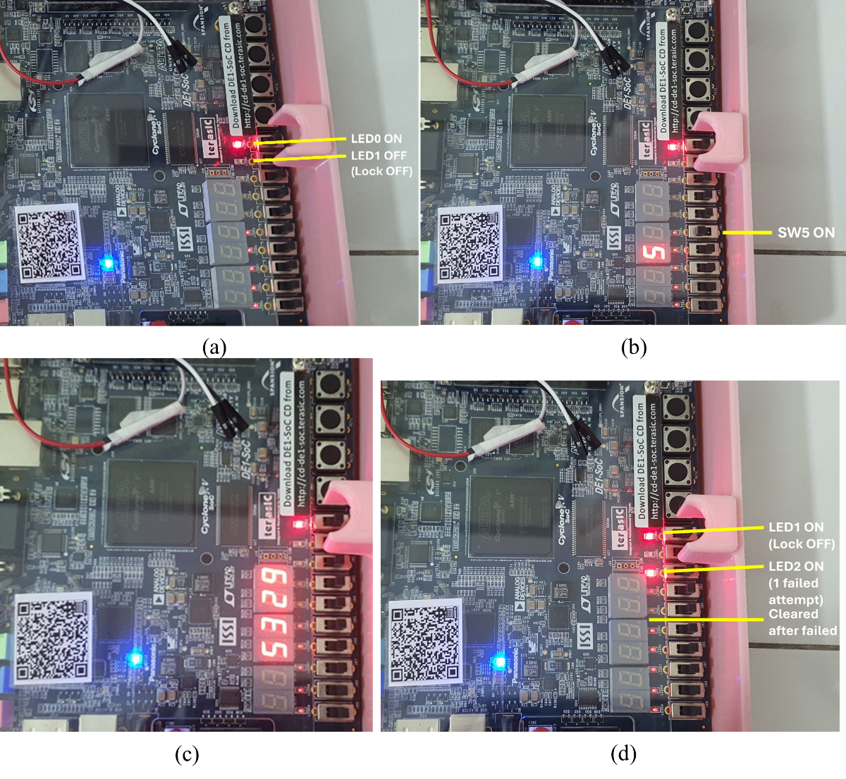
Figure 16: Hardware Testing Results of the Secure Digital Access Control System (a) idle (b) digit input using switches (example: SW5 -> digit 5) (c) full digit entry displayed on 7-segment (d) system locked state (1 failed attempt)
Each digit is entered in a particular sequence and as shown in Figure 17 (c) all the digits entered are shown clearly in all the 7 segment displays.
The onboard KEY buttons and external pushbuttons perform the same control functions, including confirm, clear, and reset. After the confirm button is pressed, the system verifies the password. A correct password unlocks the system, while an incorrect password keeps it locked. In both cases, the entered digits are cleared automatically after verification.
The failed attempt function was also verified. Each wrong password activates the buzzer and increases the failed attempt indicator using LEDR2 to LEDR4. After three failed attempts, the system enters a 15-second lockout period where no input is accepted.
The inactivity timeout was also tested successfully. If the user stops entering digits for a certain time, the system clears the input and activates the buzzer.
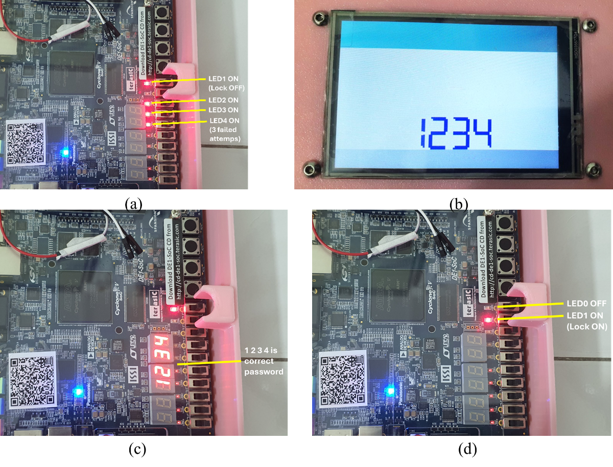
Figure 17: Hardware Testing Results of the Secure Digital Access Control System (a) 3 failed attempt and locked out for 15s (b) password display on TFT (c) correct password verification (d) system unlocked state
Overall, the hardware testing confirms that all major functions work correctly, including digit entry, password verification, automatic clearing, timeout, buzzer feedback, and lockout after three failed attempts.
5.2 Video Demonstration
Video 1: FPGA Password Lock Demo with Hidden Password Display Using Asterisk Symbols
Video 2: FPGA Secure Access Control System Demo with Keypad, TFT Display and 3D-Printed Enclosure
6 Conclusion
In conclusion, this project successfully designed and implemented a Secure Digital Access Control System using an FSM architecture on the DE1-SoC FPGA Board. The system was developed using synthesizable Verilog HDL and divided into key modules, including FSM control, Datapath, input conditioning, output control, and top-level integration.
The system performs the required functions correctly, including 4-digit password entry, password verification, automatic input clearing, inactivity timeout, and 15-second lockout after three failed attempts. Hardware testing confirmed that the FSM transitions correctly between IDLE, ENTRY, VERIFY, GRANTED, DENIED, LOCKOUT, and TIMEOUT states, while the Datapath stores digits, compares passwords, and counts failed attempts properly.
The project also demonstrates successful hardware integration inside a custom 3D-printed enclosure. Although there are minor limitations, such as slight input delay, simple buzzer feedback, and dependence on a development board, they do not significantly affect the system operation.
Overall, this project demonstrates practical understanding of FSM-based digital system design, FPGA implementation, and hardware integration.


