
Therotical Wokring
Capacitive sensors are widely used in industrial, biomedical, and consumer applications due to their exceptional metrological properties. The core sensing principle relies on changes in dielectric permittivity or electrode configuration, which facilitates outstanding performance metrics, including low noise, sub-picofarad resolution, and a compact form factor. Human-robot collaboration, temperature , pressure, and humidity monitoring are some of the applications of capacitive sensors in an industrial environment. In biomedical instrumentation, capacitive sensors are utilised for biosensor arrays, impedimetric DNA hybridisation assays, and microfluidic cell counting applications. This broad application spectrum underscores the critical need for robust readout electronics for capacitive transducers. Pertinent biosensor arrays require fF-resolution measurements of dynamic capacitance changes over extended time intervals, whereas capacitive accelerometers for human-machine interfaces demand high-speed sampling. This diverse response behaviour places conflicting design constraints on interface electronics. Consequently, the main challenges for capacitive readouts are enumerated below:
- The dynamic capacitance of a sensor may vary from a few pF to several nF, and the readout should accommodate the entire range.
- Constant sensitivity: A constant sensitivity over the measurement range ensures higher accuracy.
- Resolution: Maintaining a constant resolution is crucial to ensuring detailed, consistent measurements.
- Dynamic sensor capacitance: In numerous applications, the absolute sensor capacitance is of no relevance, and only the incremental sensor capacitance is relevant.
Let us first dive into the theoretical working of the developed system, achieving all these parameters.
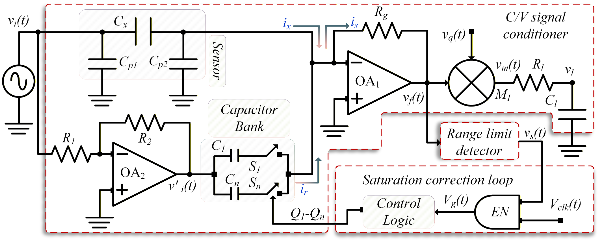
- Capacitance-to-Voltage (C/V) signal conditioner: The first stage in a measurement setup is the conversion of capacitance into a measurable quantity. In the figure above, amplifier OA1 is the transimpedance stage that provides the capacitance difference Cx- Cr. Multiplier M1 and the low-pass filter realised using Rl and Cl form the Lock-In amplifier. This section gives the voltage equivalent of the unknown capacitance difference Cx- Cr. Additionally, the lock-in amplifier removes flicker noise, yielding highly precise and accurate measurements of unknown capacitance in terms of voltage.
Range limit detector: Amplifier OA1 translates the unknown capacitance difference Cx-Cr faithfully until the voltage vf(t) is less than the saturation voltage Vcc of OA1. To achieve a bias-free capacitance measurement setup, the frontend amplifier's saturation is detected to generate a control signal for the saturation correction loop. The arrangement used to detect the peak voltage of the frontend amplifier is shown below. For a positive input, diode D1 is forward-biased (assuming no charge on Cs), and similarly, diode D2 is forward-biased. Cs charges to the peak value of vf(t) and holds this charge. This is buffered through OA4, represented as vp, and vp is the peak of vf(t). This voltage is compared with a reference voltage Vr using a comparator; when vp>Vr, vs(t) is high, indicating OA1 saturation.

Saturation correction loop: The saturation of OA1 is used to generate a control signal for the digital logic. A clock signal Vclk(t) and vs(t) are applied to the inputs of an AND (EN) gate, and the output goes high only if both signals are high. Therefore, in the range limit detector stage, if the peak voltage is less than the reference voltage, the voltage vs(t) will remain low, and no pulses will be recorded at the AND gate output. When the peak voltage exceeds the reference voltage, the comparator output vs(t) will be set high. Consequently, when the clock signal and the comparator output are high, the EN output is high. The AND gate output signal Vg(t) is used as a clock to control a 7-stage binary ripple counter in the control logic section. Each clock pulse on Vg(t) represents saturation of vf(t), and the output of the binary ripple counter increments by 1. The diagram of the digital logic controlling the switches is shown below.
.png)
The counter output pins Q1-Q7 are used to control the switches S1-S7, and these switches, in turn, are used to connect the reference capacitors to the inverting terminal of OA1, forming a binary-weighted capacitor. For the first pulse recorded on Vg(t), Q1 for FF1 is set HIGH, closing switch S1 and connecting C1 to OA1. Similarly, for the second pulse on Vg(t), Q1 is set LOW, and Q2 (for FF2) is set HIGH, opening S1 and closing S2, disconnecting C1 and connecting C2 to OA1, and so on. In this manner, the capacitor bank is programmed automatically until the signal Vg(t) does not record a new pulse, and this is possible only when vp<Vr, implying OA1 is no longer in saturation, and the product is(t)*Rg will result in a voltage vf(t) which is within the voltage headroom of amplifier OA1. Once the opamp OA1 is drawn out of saturation, the counter holds its count. Using this count, the reference capacitor value is extracted, representing coarse sampling. The remaining sensor value, which is within the allowable capacitance differenceCx-Cr, is estimated using the lock-in amplifier. The absolute sensor value Cx is calculated by summing the coarse and fine sampling steps. The detailed range adaptation algorithm and workflow of the proposed system are shown below.

Prototyping:
First, the system is validated on a breadboard. This stage is also used to test and finalise the selected components.
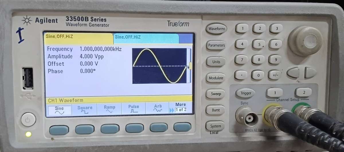
The first component, the frontend amplifier, is implemented using AD820 by Analog Devices. To saturate the amplifier at 100 pF capacitance difference (Cx-Cr), a feedback resistance of 2.5 MΩ is used. The unknown capacitance Cx is excited with a 4 Vpp sinusoidal signal at 1 kHz using an Agilent 3500B Series Waveform Generator, as shown below.
 Next, the complete lock-in path is implemented using the multiplier AD633 by Analog Devices. Once the lock-in path is verified, the range limit detector stage is implemented using TL071 and 1N5819, and the comparator for comparing the peak with the reference value Vr is implemented using TL331KDBVR. The unknown capacitance Cx is set to 100 pF, and the feedback resistance Rg is adjusted using a Bourns Trimpot to saturate OA1 at this Cx value. Also, the consequent peak value is also recorded, and the reference voltage value Vr is set to it.
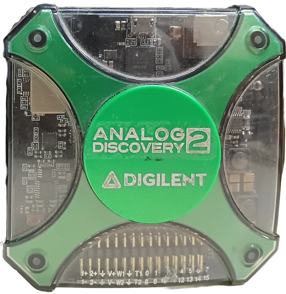
 The Gating operation is implemented using an SN74LS08N gate by Texas Instruments. TL331KDBVR output is connected to the AND Gate, and the other input of the AND gate is connected to the digital pin of an Analog Discover 2 Board, for providing the gating Clock. The image below shows an AD2 board.
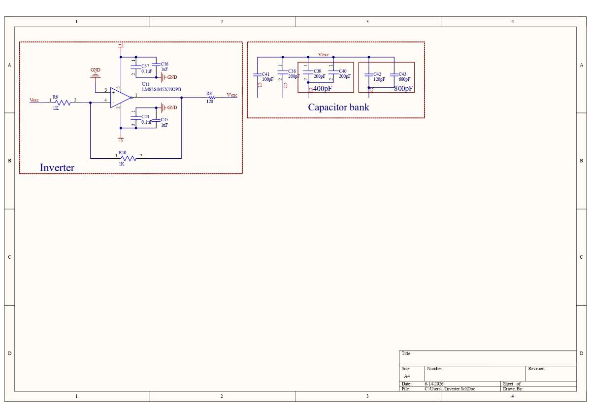
 To excite the reference capacitor bank, the excitation sinusoid is inverted using the amplifier OA2 implemented by LM8261 by Texas Instruments. This amplifier is specifically selected to ensure a large current drive. The connection of the reference capacitors to the frontend inverting terminal is made through SPST switches CD4066. The control logic is implemented using CD4024, and whenever Vg(t) goes high, the count is incremented by 1. Consequently, increasing the reference capacitor bank value Cr so that Cx-Cr< 100 pF.
 To control the ADC for fine sampling, a Nucleo board NUCLEO-G070RB by ST Microelectronics is used, as shown below.
.png)
PCB Design
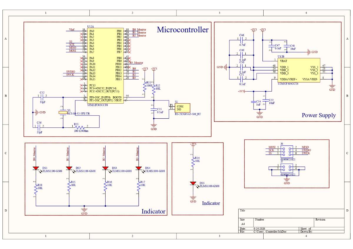
Once the breadboard prototype was working, the PCB was designed in Altium Designer. In the fabricated PCB, the STM32F303 by ST-Microelectronics was used. The microcontroller is used to control and generate the clock for the Saturation Correction Loop and the Capacitor Bank.
The PCB starts with the design of its PMU, and it uses a total of 3 LDOs. LT3032EDE-12, LT3032EDE-5, and MAX8510 for powering the complete prototype.
.jpg)
Next, the frontend amplifier with the lock-in stage and the range-limit detector stage was designed. From the schematic, it can be seen how the feedback capacitor is used with AD820 to avoid ringing.
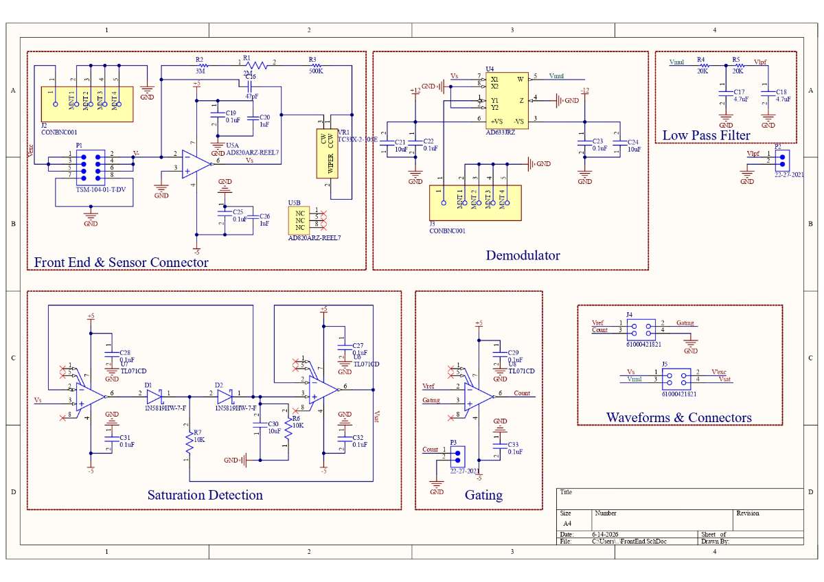
To implement the saturation mechanism, the ripple counter and the switching system is designed next.
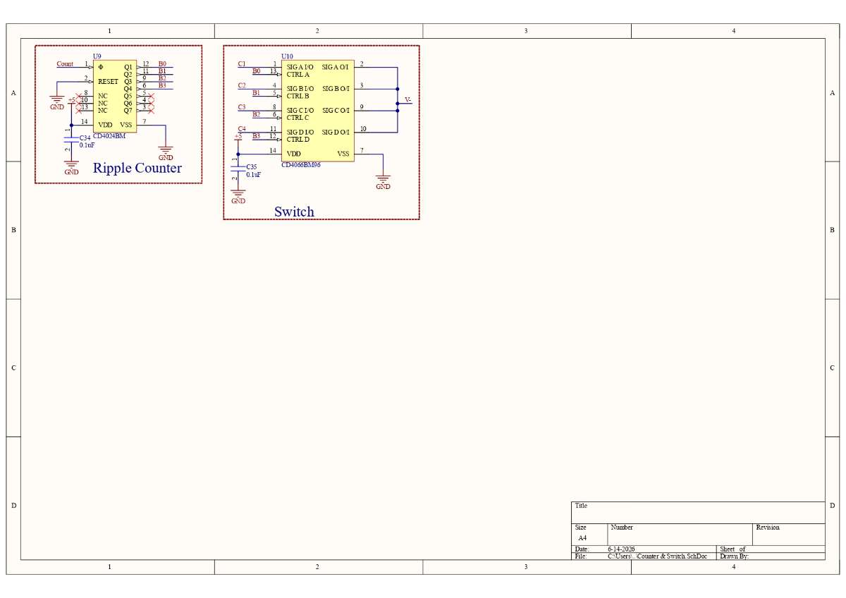
The reference capacitor bank contains 7 capacitors, since the CD4066 has only 7 lines. If a particular capacitor value is unavailable, it is implemented using a parallel capacitor connection, as shown below.
Finally, to control the onboard ADC, switching signals, and the control signals, an STM32 microcontroller is used. LEDs are used to indicate the state of the Control Logic Pins; thus, by looking at the LEDs, an estimate of the unknown capacitance can be made.
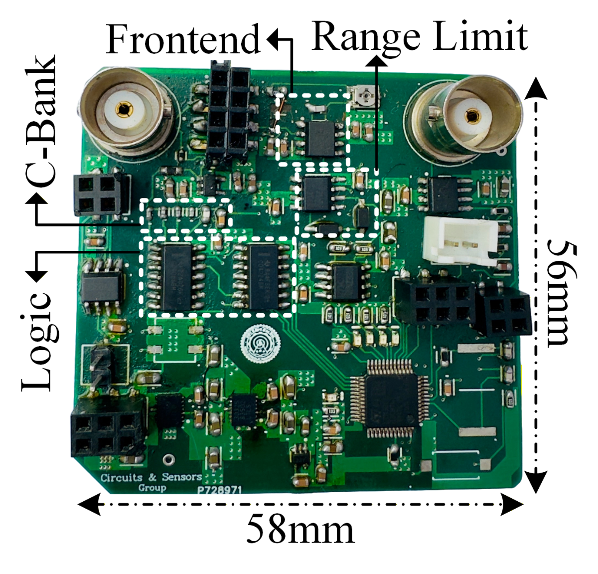
The final fabricated and soldered PCB is shown in the image below. The image highlights different sections of the working prototype.
.png)
PCB Verification & Results
The proposed system is first simulated in Multisim and then prototyped. To test the system's competency, the fabricated prototype is tested under multiple experimental conditions. The sinusoidal excitation vi(t) and the quadrature signal vq(t) are generated using a 33500B waveform generator by Agilent. The frequency of vi(t) is set to 1 kHz with a peak amplitude of 4 V, whereas vclk(t) is set to 700 Hz and generated using the onboard controller STM32F303CCT6 by ST Microelectronics. The C/V stage, including OA2 and the range limit detector, is biased at ±5 V. The EN gate, including the range-adaptation loop, operates at 3.3 V. The multiplier is biased with a GPE-4323 power supply at ±10 V, and all other voltages are derived from it via an onboard power module. The values of R1 and R2 are 1 kω. The feedback resistance Rg is 2.5 MΩ, whereas Rl and Cl are 20 kΩ and 4.7 µF, respectively. Similarly, Rf is 1 kΩ, and Cs is 10 µF. A MOSFET Q1 is used to reset the saturation detection capacitance Cs at every high pulse on Vg(t). Discrete and precise capacitors and resistors are used to emulate the behaviour of a capacitive sensor and its leakage resistance, respectively. The LCR meters 4910 by Aplab and ZM2376 are used to approximate the actual values of the various discrete passive components employed.
Capacitor bank design:
The architecture of the programmable reference capacitor bank is designed based on the maximum allowable capacitance difference that the frontend amplifier can accommodate without saturation (for the given value of Rg), along with the number of available reference states in the system (depending on the number of states in the control logic). Under these constraints, the interface is specified for a total operational range of 1 pF to 12.8 nF. The achievable measurement range is therefore not constrained by the bias voltage, but is instead determined by the programmable reference bank and the saturation detection mechanism. Furthermore, the range is inherently scalable, as the total measurement span can be programmed by increasing or decreasing the number of binary-weighted capacitors in the bank. The selected bin width is determined by the application's range and resolution requirements and can be programmed accordingly without altering the underlying architecture.
The capacitor bank consists of seven reference capacitors C1-C7, with values 100 pF, 200 pF, 400 pF, 800 pF, 1.6 nF, 3.2 nF, and 6.4 nF, respectively. The capacitors are connected to OA1 via switches S1 through S7. These switches are controlled by the 7-stage ripple counter output pins Q1 to Q7, and for any change in the count, the equivalent reference capacitance is adjusted accordingly, making the combination a binary-weighted capacitor. Consequently, Cr tracks Cx through the range limit detector and the saturation correction subsystems. The amplifier OA1 is designed such that it saturates to Vcc for DeltaC=100 pF. When OA1 saturates, vp>Vr and vs(t) goes high. Eventually, Vg(t) sets high, incrementing the count by 1 (Qi(n+1)) and connecting a succeeding reference capacitor to OA1. This process continues until the condition vp>Vr is met, and with every pulse on Vg(t), the count is incremented, further closing the switches intrinsically and increasing the equivalent value of Cr. As soon as vp<Vr, there are no new pulses on Vg(t), signifying that the difference between Cx and Cr (Delta C) is less than 100 pF. Therefore, for any value of Cx till 12.8 nF, the maximum allowable capacitance difference (Cx-Cr) is 100 pF.
Results:
A. In the first experiment, the sensor capacitance is manually set to 5 nF, which causes the RLD stage to flag the correction loop, pass a high to the binary-weighted counter, and count a 1, incrementing the capacitor bank value by Co. This process continues till the RLD flag is not low and is only possible when the frontend amplifier voltage is less than saturation. This can be seen in the image around the 120 ms time stamp, where the digital lines are 0110010 (MSB first) and the cap-bank holds a value of 5 nF, making Cx-Cr<100 pF and bringing OA1 out of saturation. The resulting digital and analog signals are shown below.
.png)
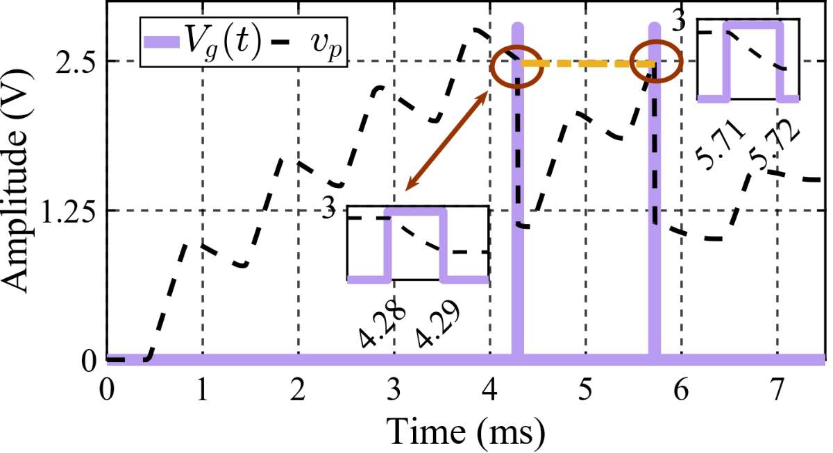
B. To assess the operation of the range-limiter detection stage, the unknown capacitance Cx is varied from 1 pF to 240 pF, and the clock signal Vclk(t) is set to 1 kHz. The voltage vp is monitored using the analog input pin on the Analog Discovery 2 board, and the signal Vg(t) is monitored using the digital pin on the same device. From the figure below, it can be seen that as Cx increases, vp increases, and when Vr is breached, the AND gate EN is triggered, causing Vg(t) to go high, turning on Q1 and rapidly discharging Cs through Q1. This arrangement ensures that the range-limiter detection stage can be employed with a high-frequency Vclk(t) without causing false triggering.
C. The range-resolution tradeoff is one of the most inherent impediments for a measurement system. However, for the proposed range-adaptable system, achieving enhanced range with a constant resolution is possible. To this end, 500 data points are collected when Cx=90 pF at various coarse sampling values. Using these values, the median resolution is 2.01 fF across the entire measurement range. Further, deviations of individual resolutions are plotted against the median resolution, and a maximum deviation of 0.28 fF is recorded over a measurement range of 12.8 nF, as shown in the figure below. An increase in deviation in the nF capacitance range can be attributed to the increased load current supplied by OA2, required to drive the capacitor bank Cr.
.png)
D. While testing the fabricated prototype waveforms at different nodes of the system, they were verified using a Agilent Oscilloscope. The image shows the resulting waveforms: the first is the excitation, and the second is the frontend amplifier voltage. The DC waveform is the extracted peak, and the last signal shows the demodulation or the working of the CV stage. It should be noted that the waveforms are collected once the digital loops have settled.
.png)
The working of the system can be found on this link: