
INTRODUCTION AND OVERVIEW
The title "Analog and Digital Communications Learning Trainer Utilizing Low-Frequency PC-Based Oscilloscope as Display" might be a long name. That is why I decided to create a "code-name" or a nickname for this project which is PAYAPA-14. "Payapa" is a Filipino word for "Peaceful". Since currently, we all facing a COVID pandemic, this is what is deprived of most of us. So I named it after the hope that we are all looking for. Also, once you have finished reading this article (or even creating it on your own), you will have peace over the knowledge in Electronics Communications since the basis of Wireless Transmissions both analog and digital are all featured here. You will also see the waveform of different signals in wireless transmission having a "Peaceful" and beautiful pace. The number 14 stands for the 14 different circuit designs found in the project; (1) 100Hz and (2) 1kHz Sine wave oscillator, (3) 50Hz/100Hz and (4) 500Hz/1kHz Square wave oscillator, (5) Full Carrier Amplitude Modulator, (6) Suppressed Carrier Amplitude Modulator, (7) Frequency Modulator, (8) Amplitude-Shift Keying, (9) Frequency-Shift Keying, (10) Phase-Shift Keying, (11) Pulse-Width Modulator, (12) Natural Pulse-Amplitude Modulator, (13) Flat-Top Pulse-Amplitude Modulator, and (14) Pulse-Position Modulator. Does my reasoning for naming this project make sense? Well, whether or not the explanation or the name is valid for you, this project would help you in understanding the very foundations of wireless communications which is a topic under Electronics Engineering, Communications Engineering, or alike. So let's get started.
CONTENTS
A. Prerequisites
- EFY's Oscilloscope
- Multisim
B. Circuit Building
- Oscillators
a. 100Hz Sine wave oscillator
b. 1kHz Sine wave oscillator
c. 50Hz/100Hz Square wave oscillator
d. 500Hz/1kHz Square wave oscillator - Analog Modulation
a. Amplitude Modulation (DSBFC, DSBSC)
b. Frequency Modulation - Digital Modulation
a. Amplitude-Shift Keying
b. Frequency-Shift Keying
c. Phase-Shift Keying - Digital Transmission
a. Pulse-Width Modulation
b. Pulse-Amplitude Modulation (Natural, Flat-Top)
c. Pulse-Position Modulation - Auxiliaries
a. Offset Selector
b. Supply
C. OUTPUT
A. PREREQUISITES
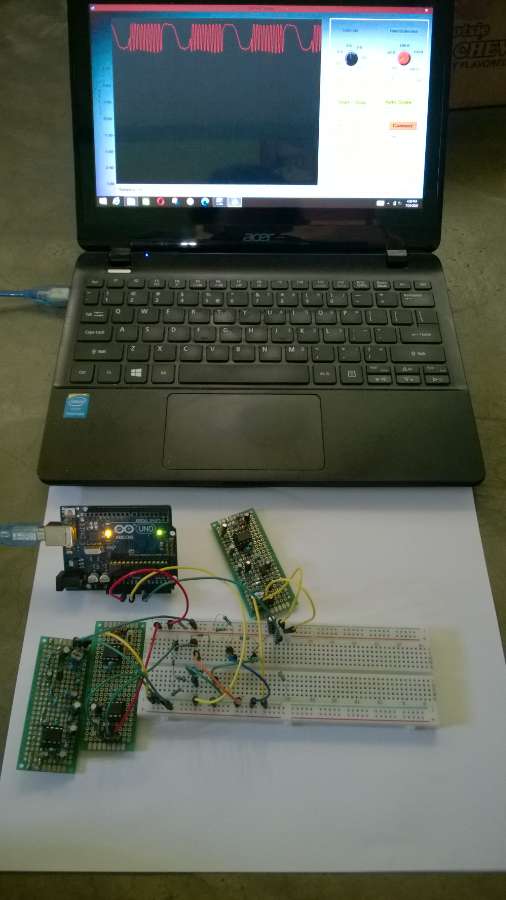
1. EFY's Arduino Oscilloscope
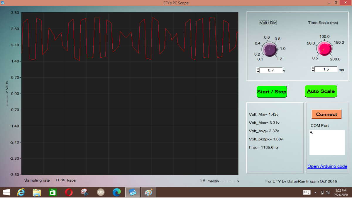
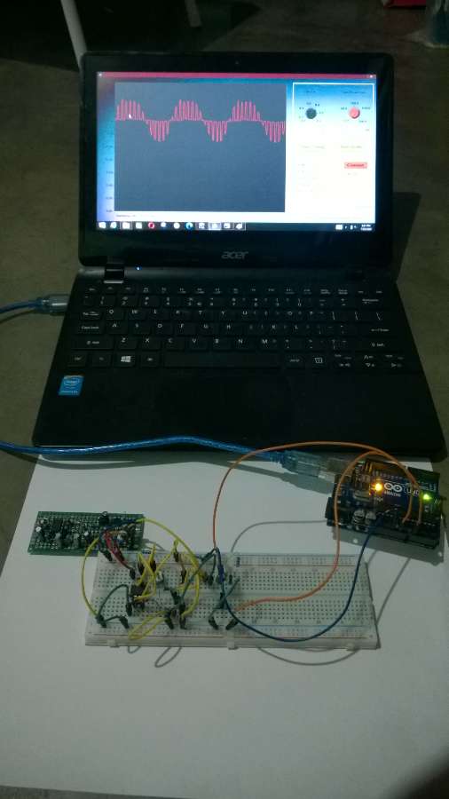
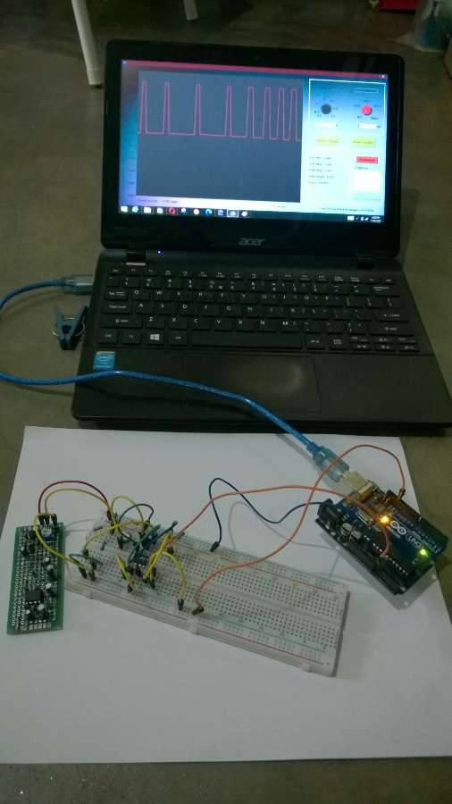
In order to see the waveform, you need an oscilloscope. All licensed-free and low-frequency PC-based scopes will do since the frequency range of our project is in Audio frequency only specifically, 50Hz to 2kHz only.
Although you can use other PC-based oscilloscope for this project, I find EFY's Oscilloscope well suited for Payapa-14 so I implemented it here. You can download the software in the link below:
https://www.electronicsforu.com/electronics-projects/pc-based-oscilloscope-using-arduino
All instructions in the software installation and use are written in there.
2. Multisim (Preferred, but not required)
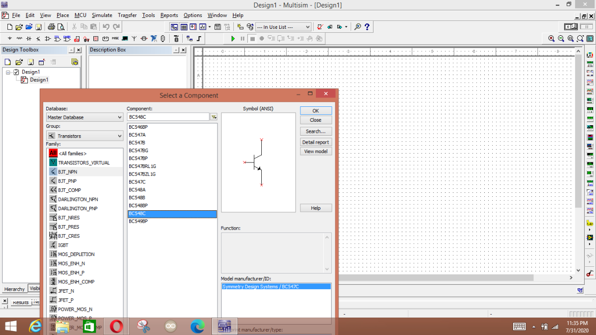
Multisim was used as a simulation tool in each circuit of Payapa-14. Simulation is very important especially for large and complex systems. Simulation is explained a lot more in the proceeding sections.
Installation and purchase of Multisim Desktop Application can be found using this website:
https://www.ni.com/en-ph/support/downloads/software-products/download.multisim.html
The version of the software I have is 12.0, although 14.2 is already available in the National Instruments website.
B. CIRCUIT BUILDING
Before proceeding in the circuit building part, let us first examine the effective circuit designing steps of any circuit. I have list down five steps that I used in building this project, but for recreating this project, you will only need the last three of them. These are personally used by me over the past few years in Electronics Engineering.
Circuit Designing Steps:
Step 1: Circuit Design Theory
Circuit Design Theory is when a designer will attempt to use the basic theories in Electronics. Example is when designing a Common Emitter Amplifier, in which mathematical approaches might be necessary. I also call this step a "Scratch paper method" since often time the designer draws the schematic in a piece of paper.
Step 2: Simulation
Simulation means imitation of situation or process. This step is important especially in large systems and in designs which processes or outputs signal such as in Wireless communications. Simulation allows the designer to verify the output quickly. This step saves time, effort and money as well. Payapa-14 used Multisim in the design simulation.
Step 3: Circuit Testing
Once the desired output is achieved on simulation, the circuit can be tested using the actual devices. Often case, simulation reflects the actual behavior of the circuit with a little discrepancies. The error in simulation varies depending upon the complexity of the circuit or with the simulation tool.
Step 4: Troubleshooting
Troubleshooting is necessary in finding the error from simulation or if no simulation, in the design. The length of troubleshooting time depends upon the severity of error or in the complexity of circuit itself.
Step 5: Design Revision
After the error has been found, necessary correction in the original design can be made. The Step 3 must be performed again in order to see if the error is minimized or addressed. If not, the Steps 3-5 needs to be done over again.
Circuit Building Part 1: The Oscillators
The Payapa-14 Consists of 4 Oscillators: 100Hz and 1kHz sine wave, and 50Hz/100Hz and 500Hz/1kHz Square Wave. These are necessary because they will serve as Carrier (Modulation signal) or Information (Modulating Signal) for the rest of the circuits.
a. 100Hz Sine wave oscillator
b. 1kHz Sine wave oscillator
c. 50Hz/100Hz Square wave oscillator
d. 500Hz/1kHz Square wave oscillator
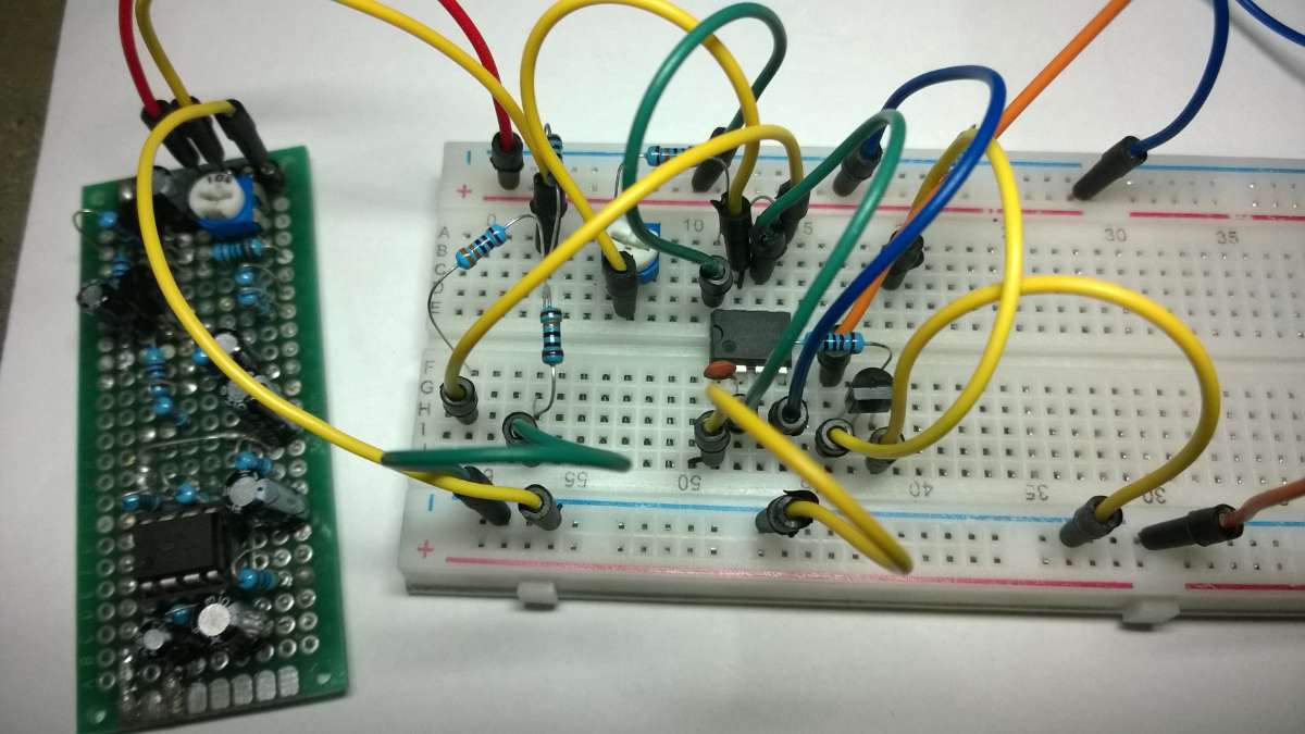
a. 100Hz Sine Wave Oscillator
The Circuit:
.jpg)
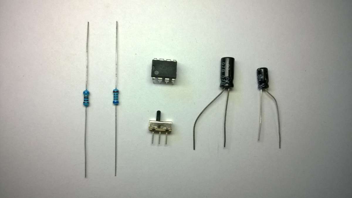
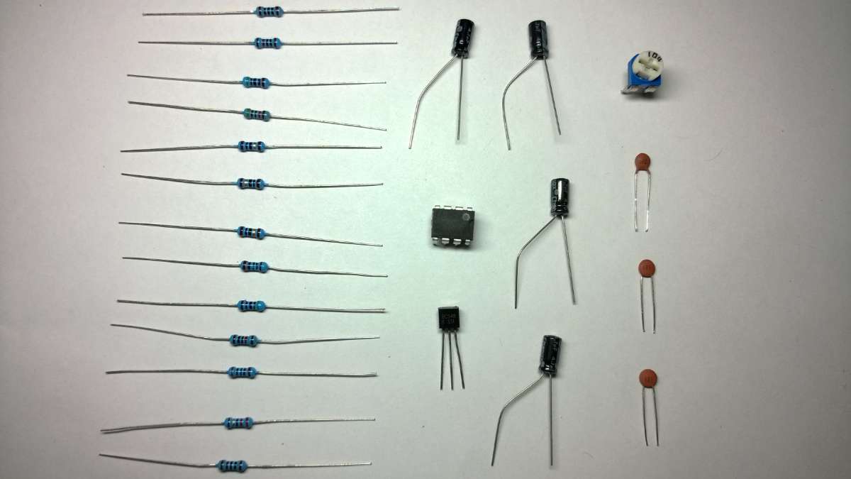
Components:
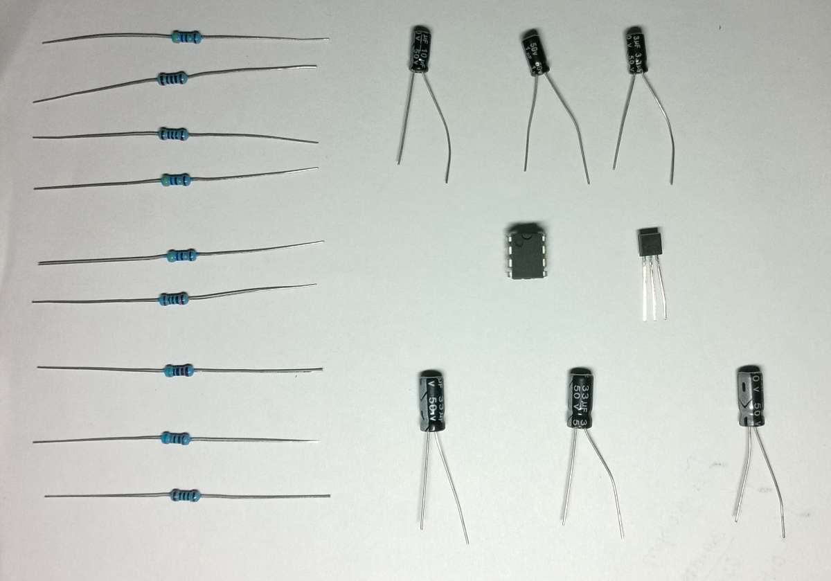
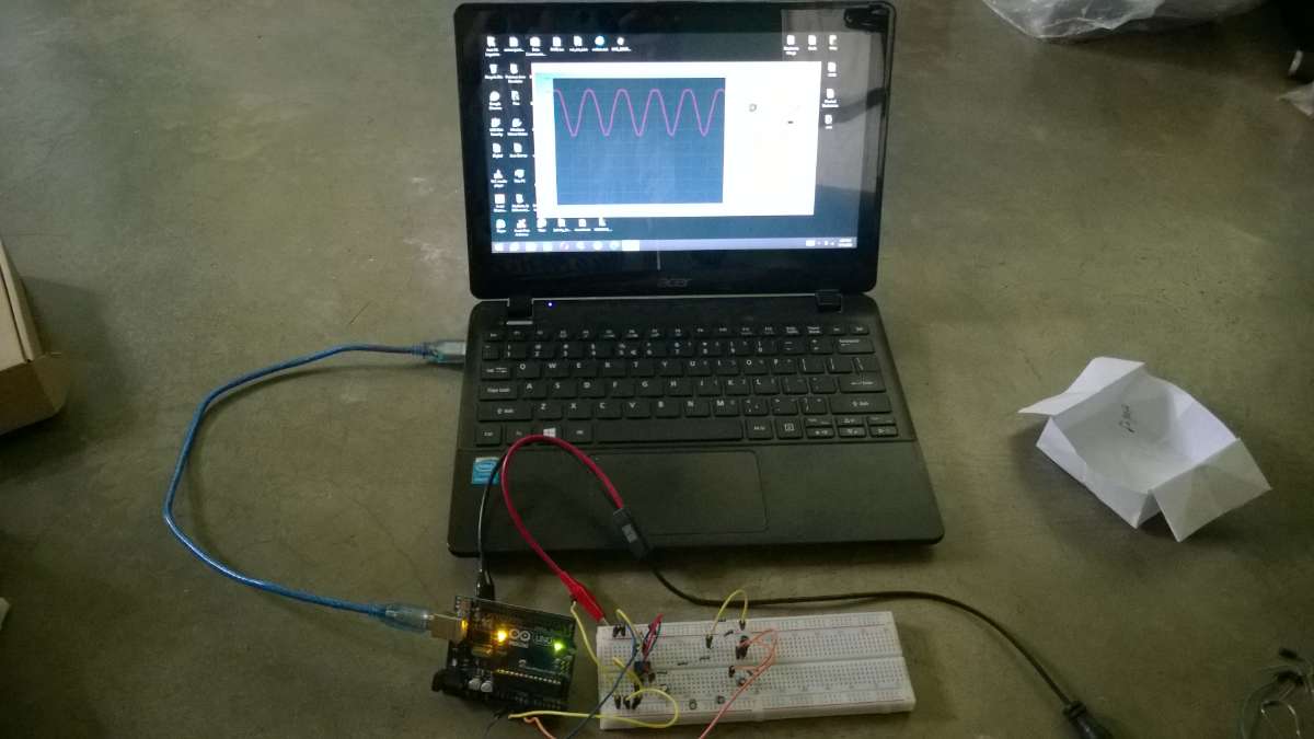
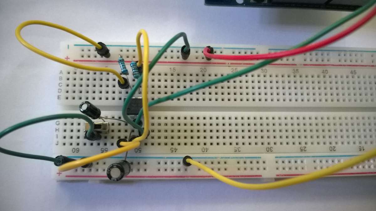
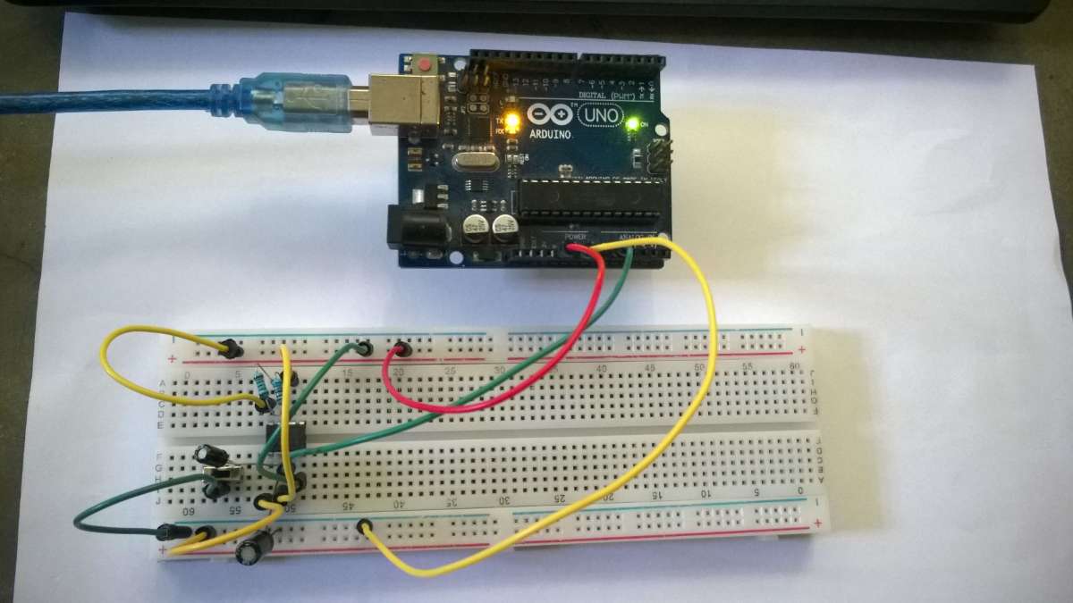
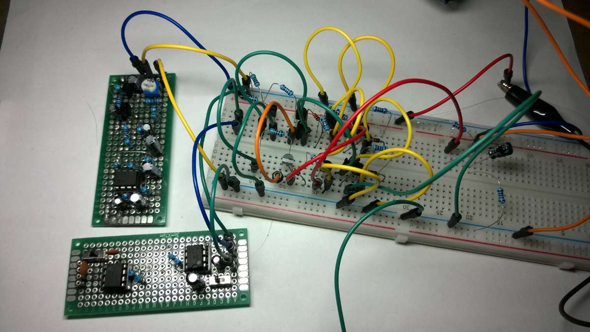
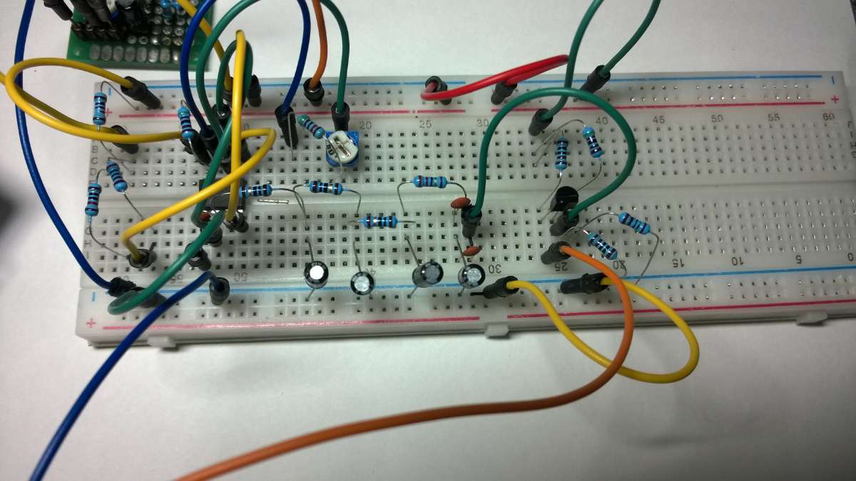
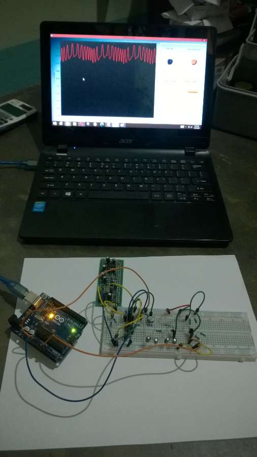
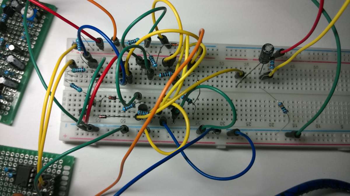
Once the components above are gathered, connect them in a breadboard to test the output. Follow the connection on the circuit and you must have connected them like this:
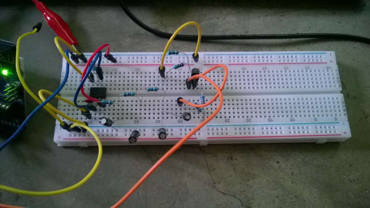
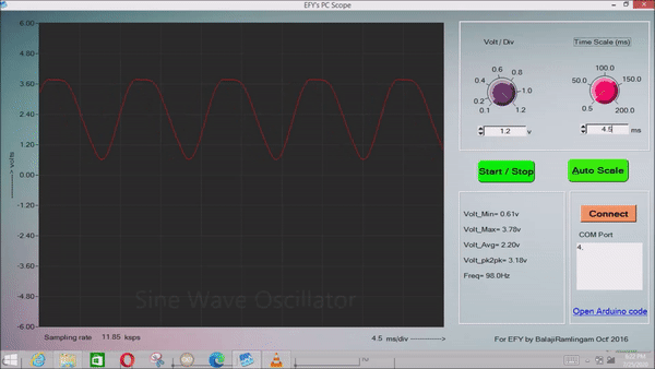
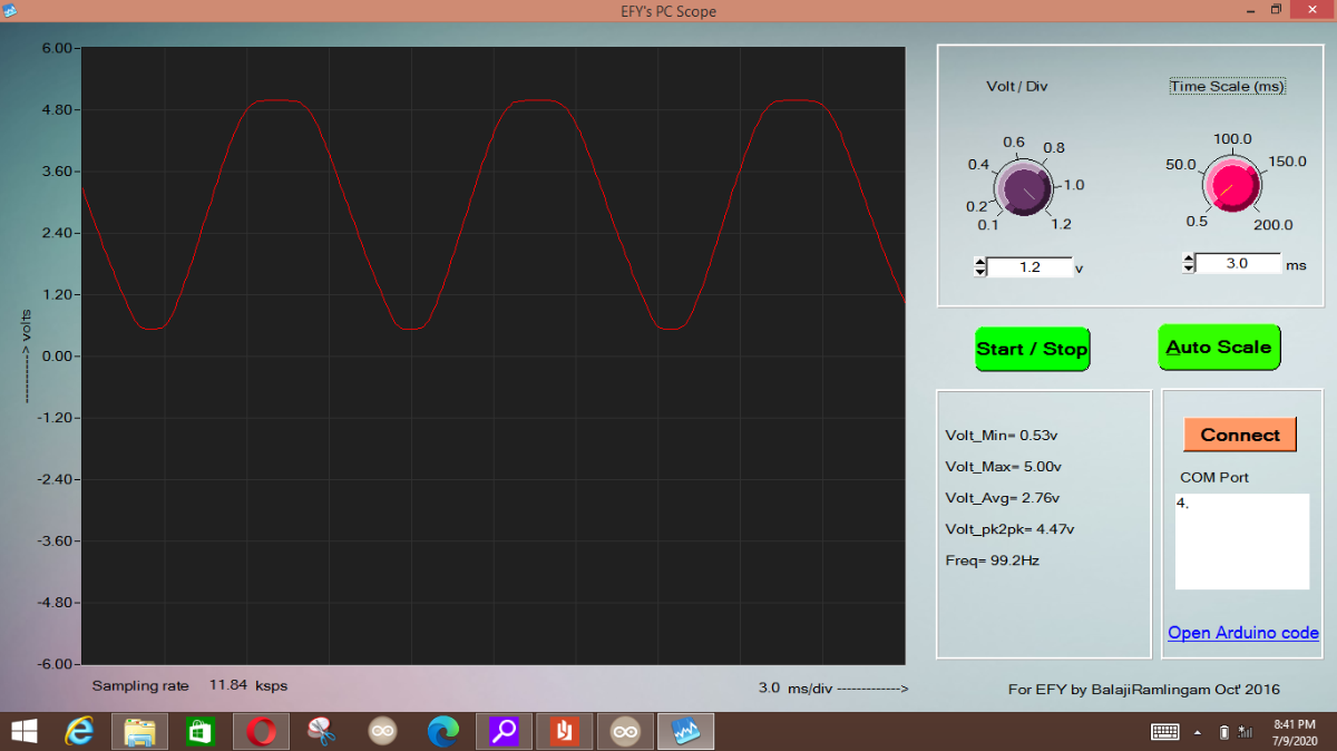
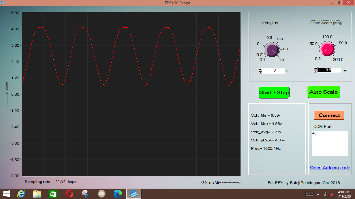
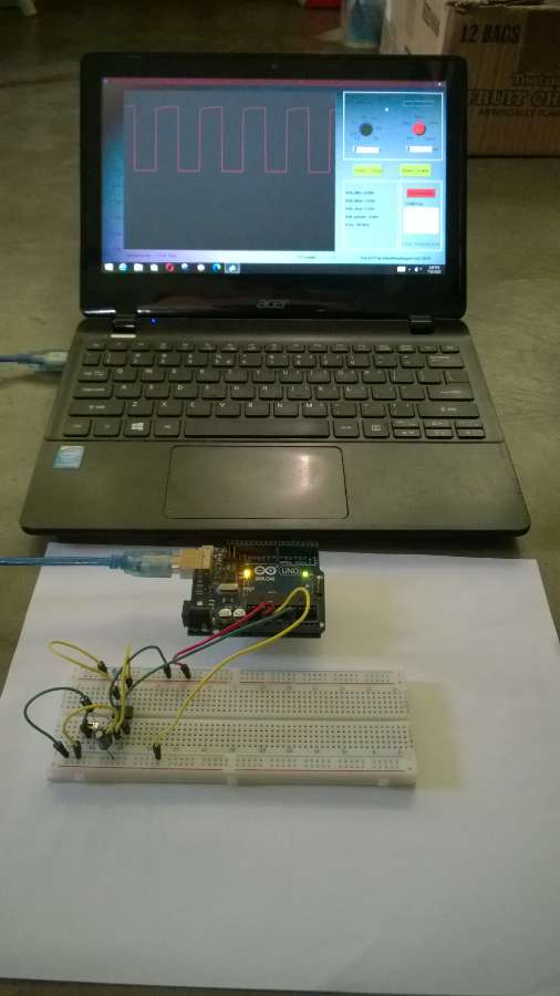
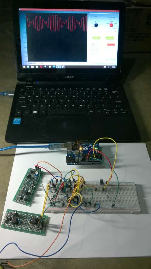
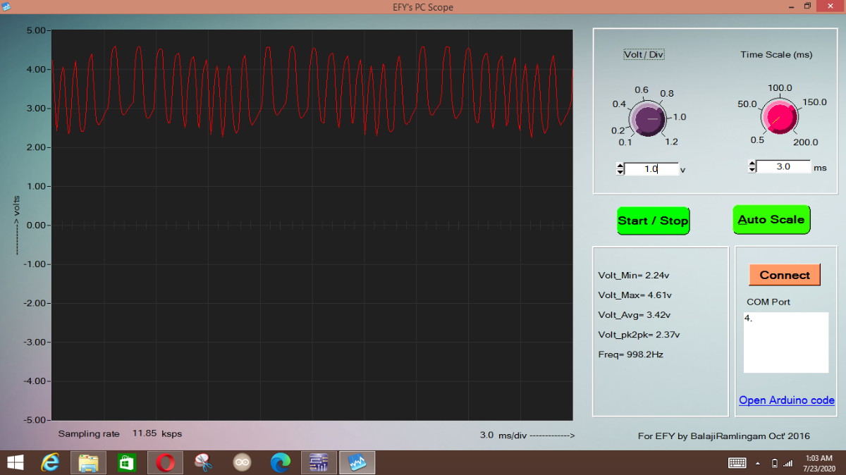
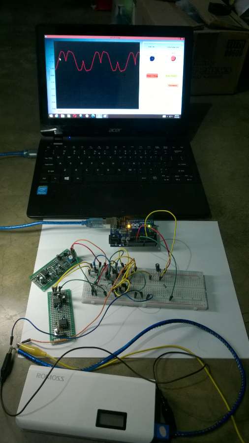
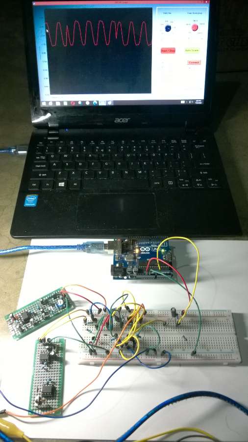
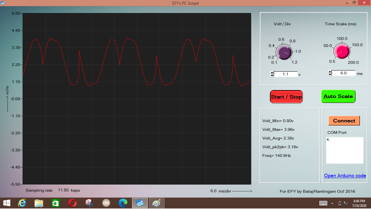
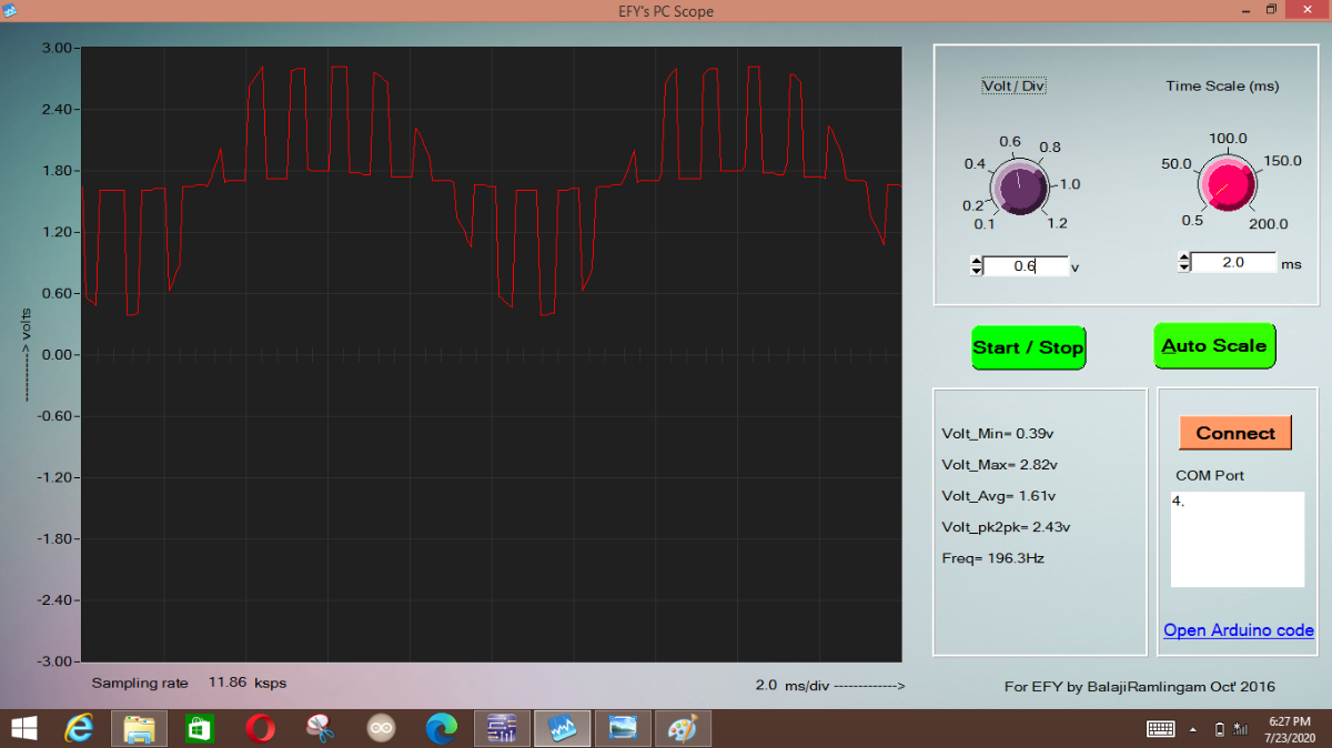
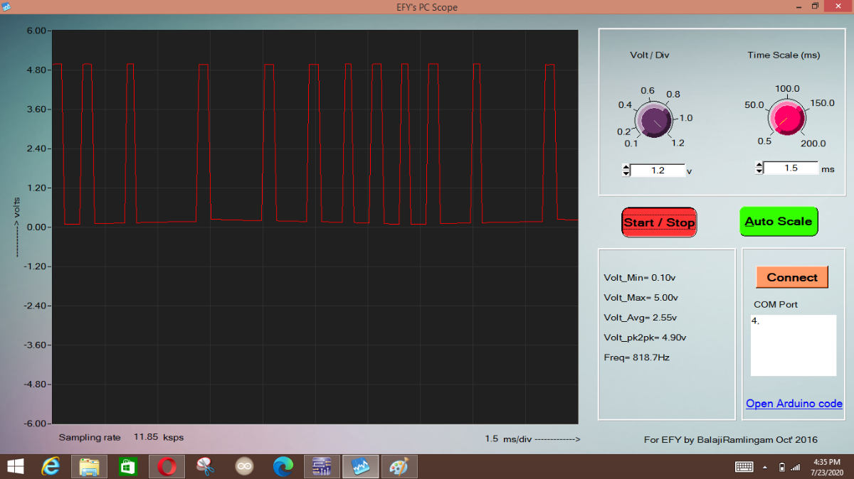
Connect your Arduino with the pcscope code uploaded in it. Run the EFY's Oscilloscope and check the output waveform in which you must get a signal like one below:
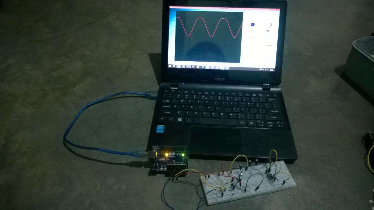
Screenshot:
b. 1kHz Sine Wave Oscillator
The Circuit:
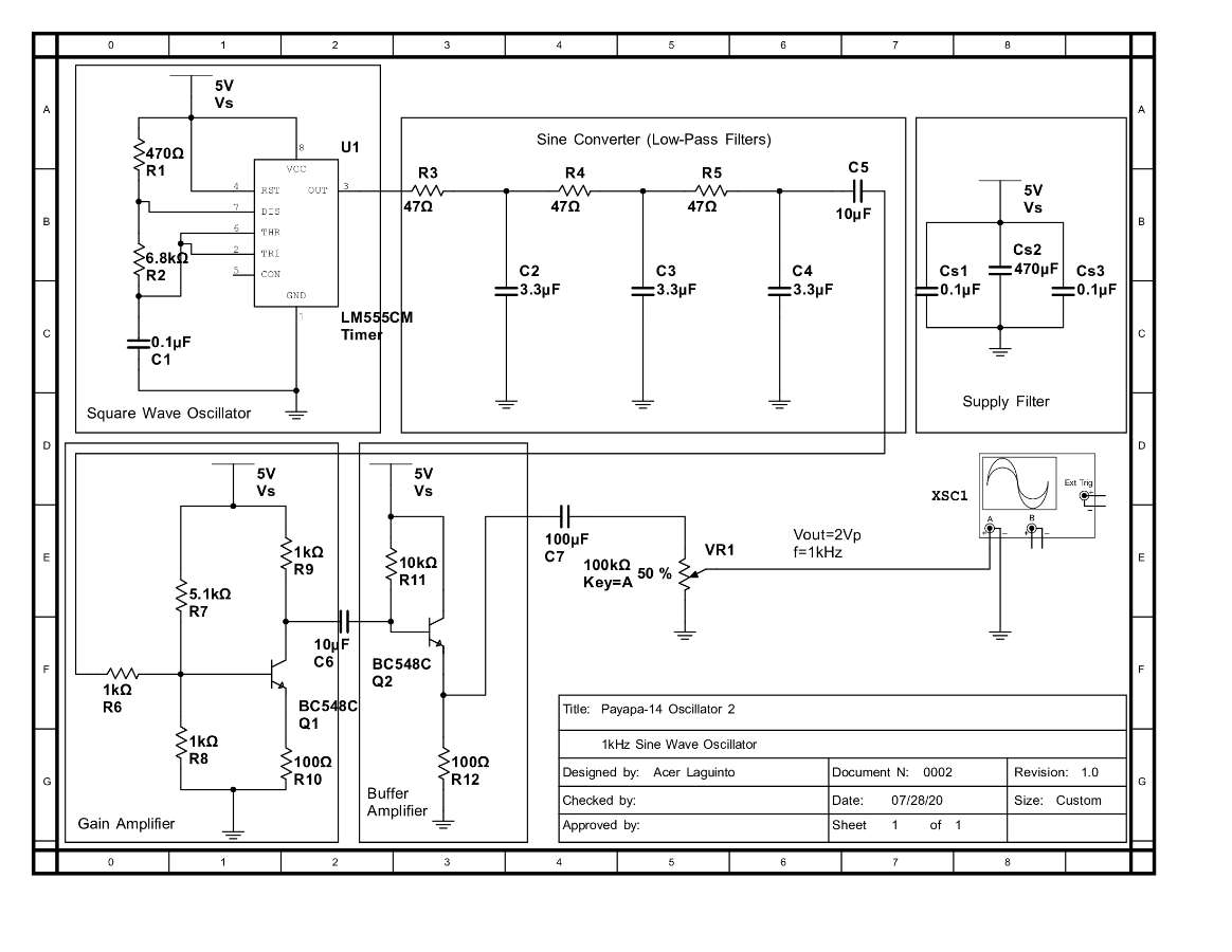
Components:
.jpg)
The output waveform should be:
Screenshot:
c. 50Hz/100Hz and d. 500Hz/1kHz Square Wave Oscillator
The Circuit:
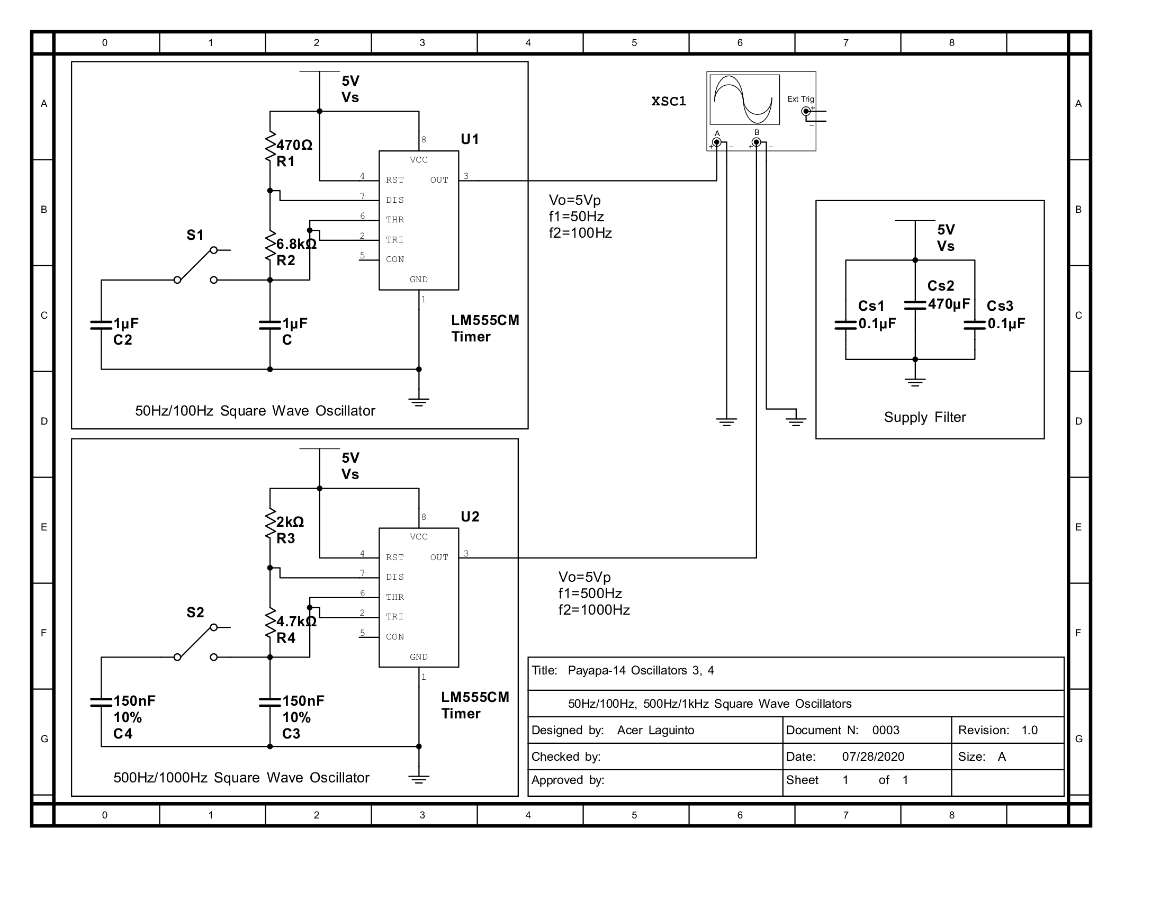
Components:
In the breadboard:
As a whole it should look like:
Check the waveform and you must get:
Circuit Building Part 2: The Analog Modulation Circuits
a. Full Carrier Amplitude Modulator (AM-DSBFC)
b. Suppressed Carrier Amplitude Modulator (AM-DSBSC)
c. Frequency Modulator (FM)
The Analog Modulation Depicted in this project is the three most fundamental ones: Amplitude Modulation (DSBFC), Amplitude Modulation (DSBSC), Frequency Modulation.
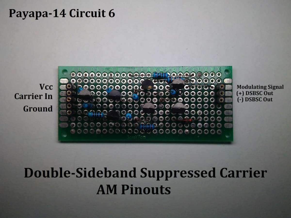
DSBFC Means Double-Side Band Full Carrier which means that the carrier power is 100% Present; Otherwise, DSBSC Means Double-Side Band Suppressed Carrier which means that the Carrier power is suppressed in the signal.
a. Full Carrier Amplitude Modulator (AM-DSBFC)
The Circuit:
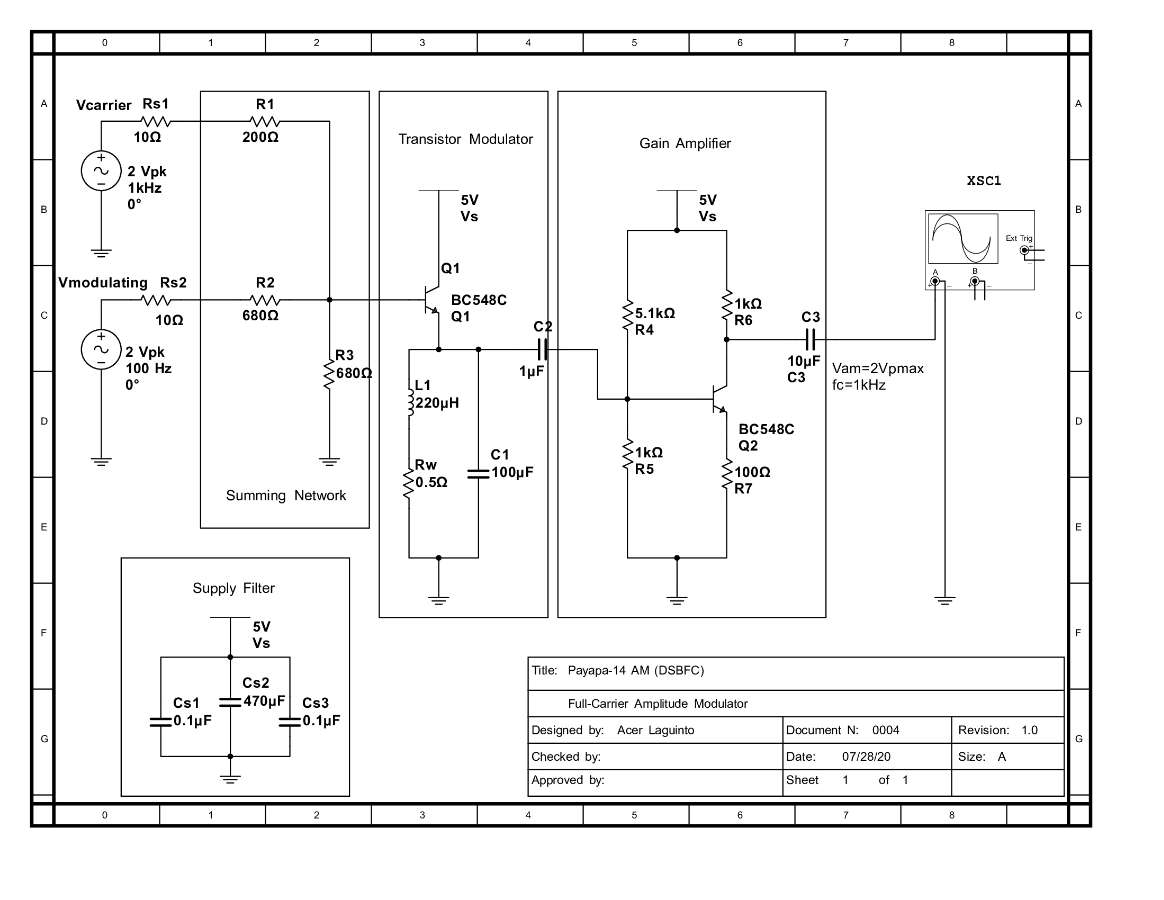
The AM Modulator used in this circuit is a transistor modulator. The Transistor Provides the sufficient detector and the amplifier is coupled with a tank circuit in order to "fill" the missing cycle of the wave creating an AM output.
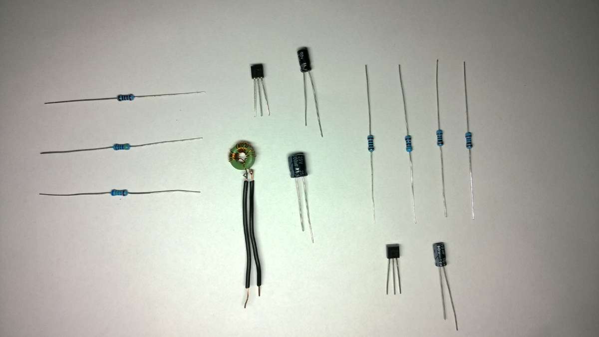
Components:
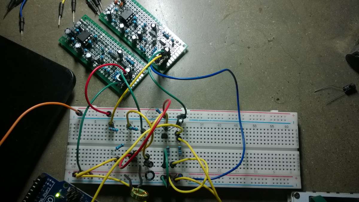
Connect the components in the breadboard as shown:
Again, using EFY's Oscilloscope, you should get an output waveform like this:
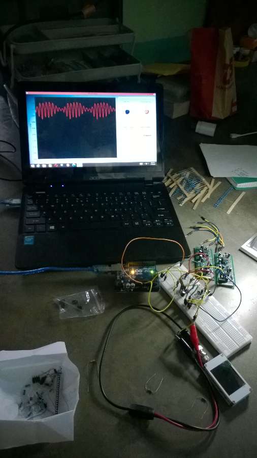
Screenshot:
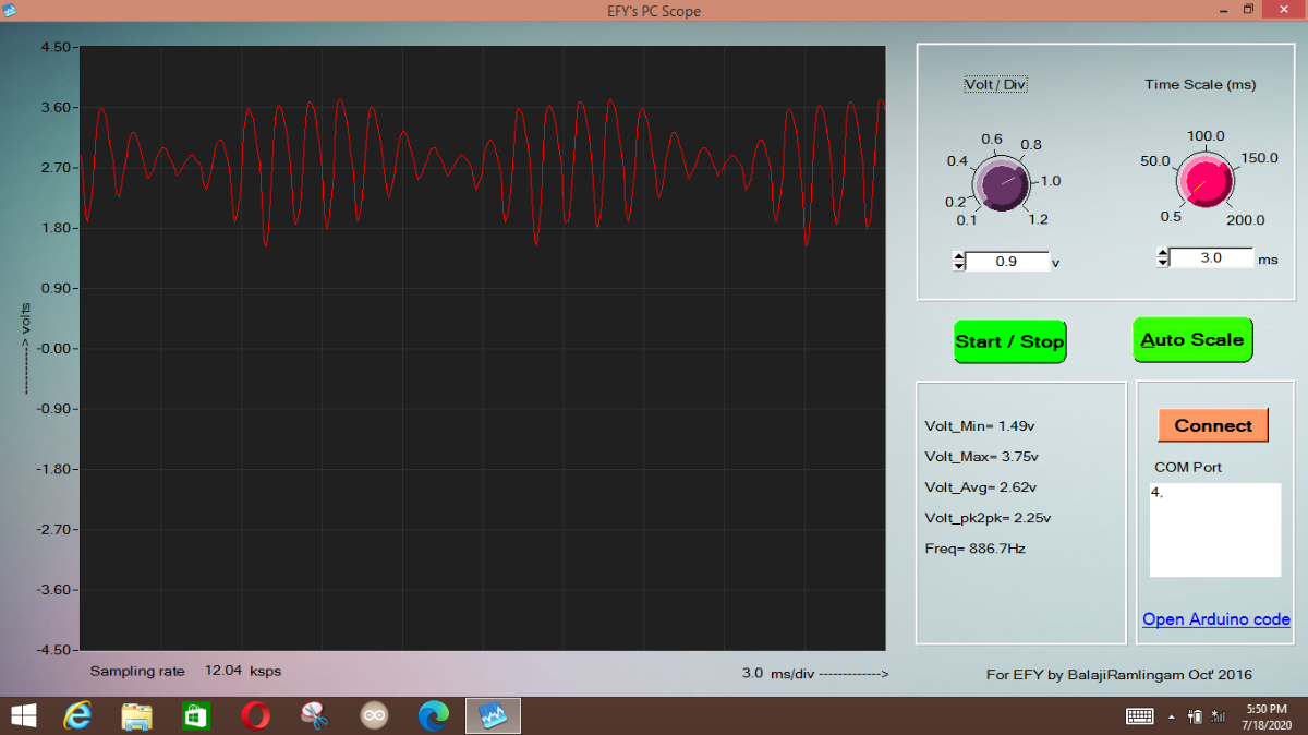
b. Suppressed Carrier Amplitude Modulator (AM-DSBSC)
The Circuit:
The DSBSC is a special circuit of AM in which the Power in the Carrier is suppressed. The circuit is:
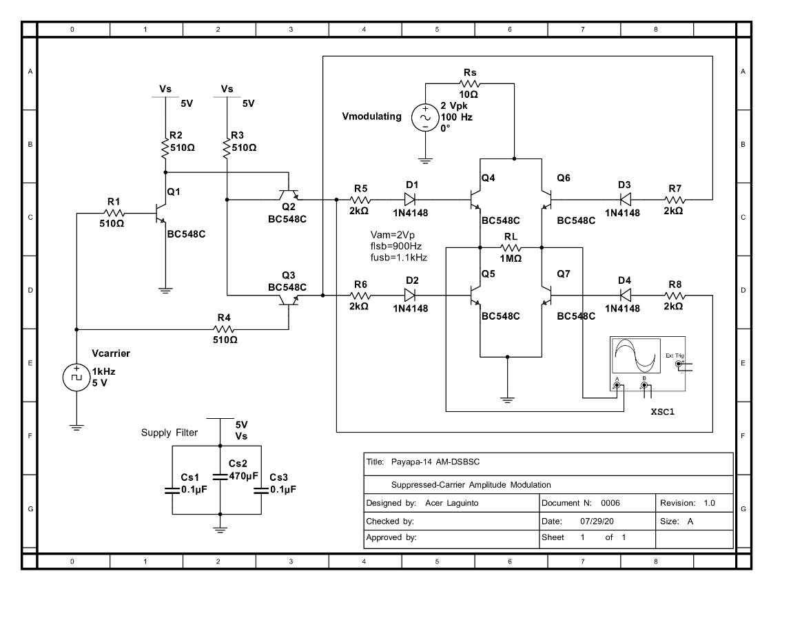
In actual, a bandpass filter of center frequency equal to the carrier frequency is placed at the output stage
Components:

Connect the components in a breadboard to test the output. Use the 100Hz sine wave you have created previously as the modulating signal input, and the 500Hz/1kHz Square wave oscillator as the Carrier input.
The output of the circuit should be:
Screenshot:
c. Frequency Modulator (FM)
The Circuit:
.jpg)
Components:
Connect the components properly in a breadboard following the schematic above just like this:
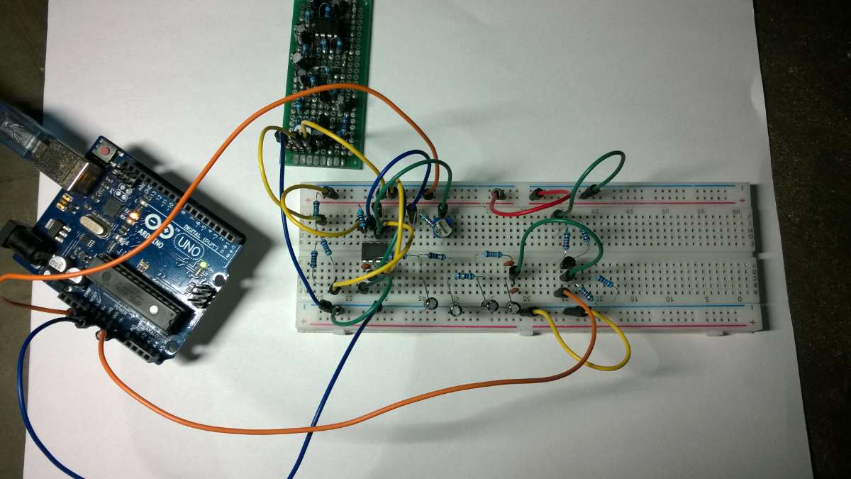
Use the 100Hz sine wave as input signal so the entire circuit connection will look like this:
In which the output signal should be:
The screenshot of the output waveform:
Circuit Building Part 3: Digital Modulation
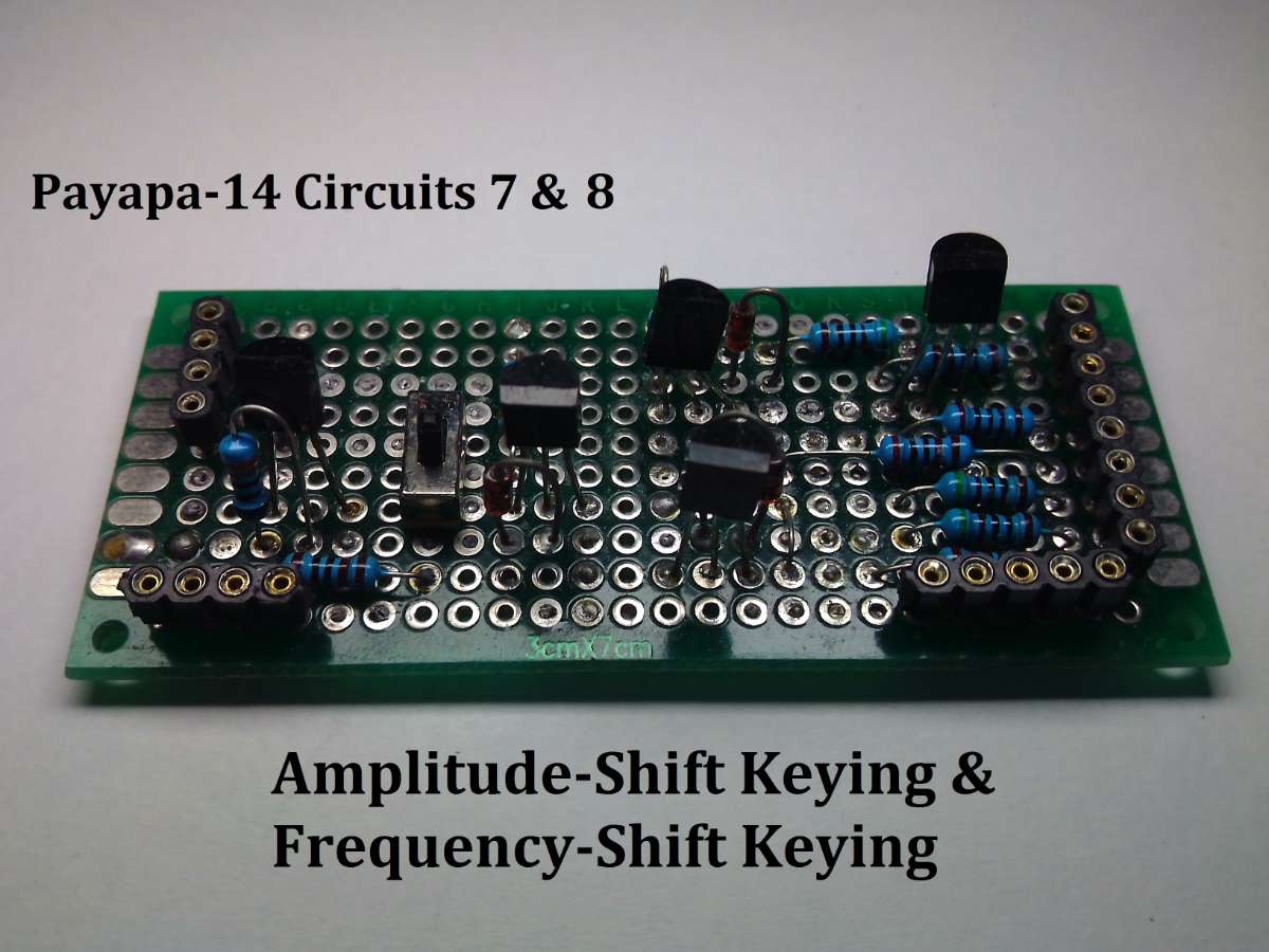
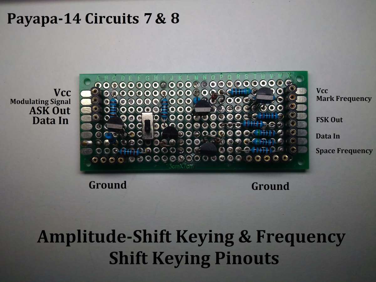
a. Amplitude-Shift Keying (ASK)
b. Frequency-Shift Keying (FSK)
c. Phase-Shift Keying (PSK)
There are Primarily three fundamental Modulation Techniques in Digital Modulation, namely; Amplitude-Shift Keying (ASK), Frequency Shift Keying (FSK), and Phase-Shift Keying (PSK). Digital Modulation techniques are very essential in modern-day wireless communications circuits because they allow the digital signals to be transmitted in the free space.
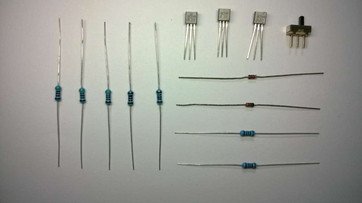
a. Amplitude-Shift Keying (ASK)
The Circuit:
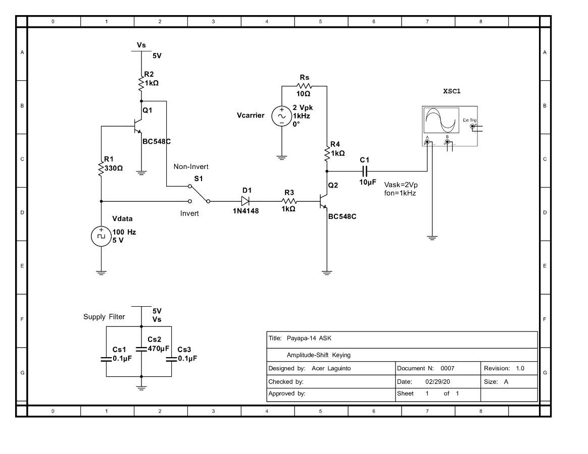
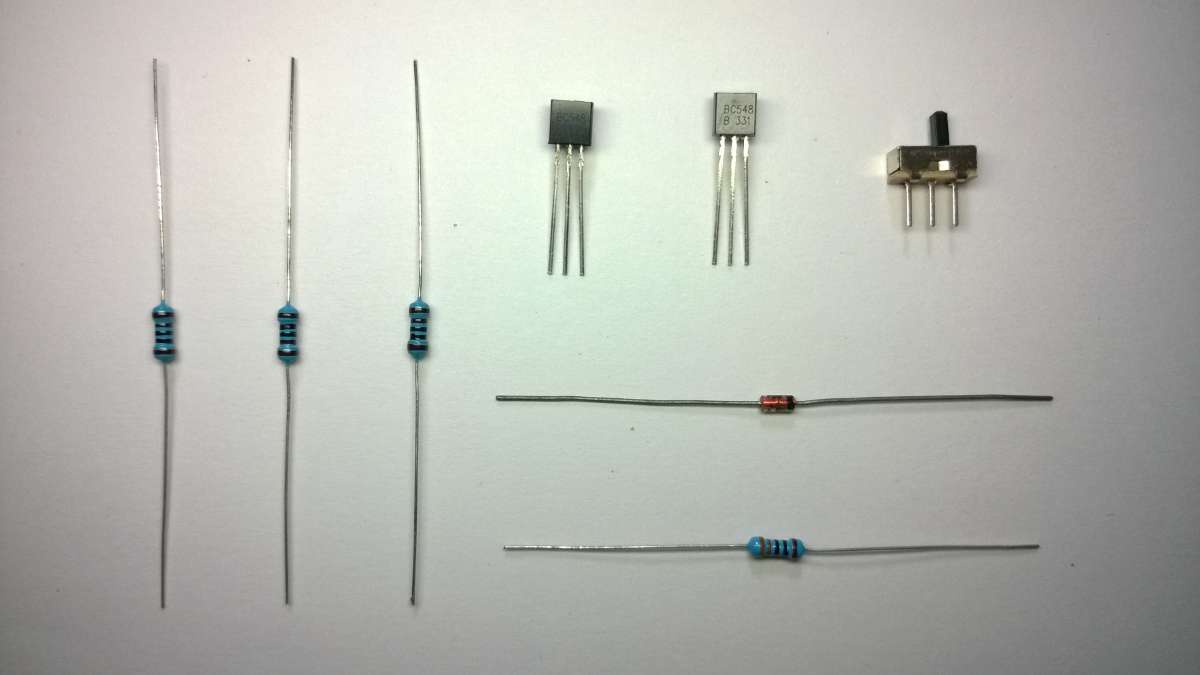
Components:
Connect them in a breadboard as shown:
Use the 1kHz sine wave oscillator as the carrier and the 50Hz/100Hz Square wave oscillator as the modulating signal. Connect the A0 of the arduino the the output of the ASK and you should be able to get the waveform below:
The screenshot of ASK Waveform:
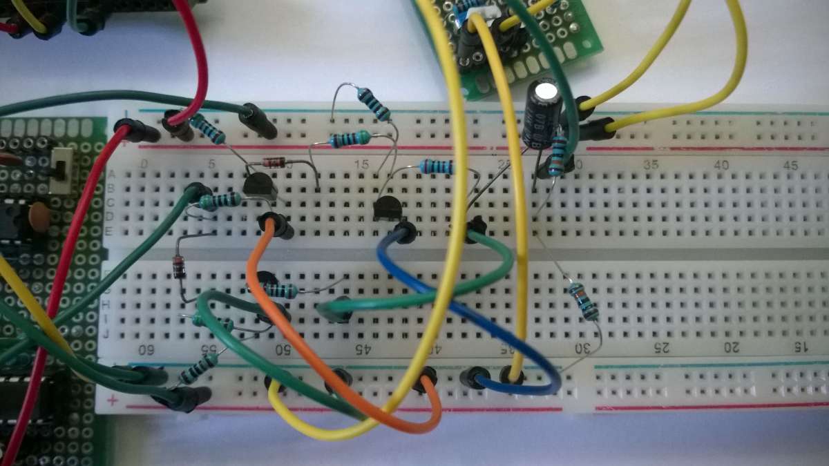
b. Frequency-Shift Keying (FSK) Circuit
The Circuit:
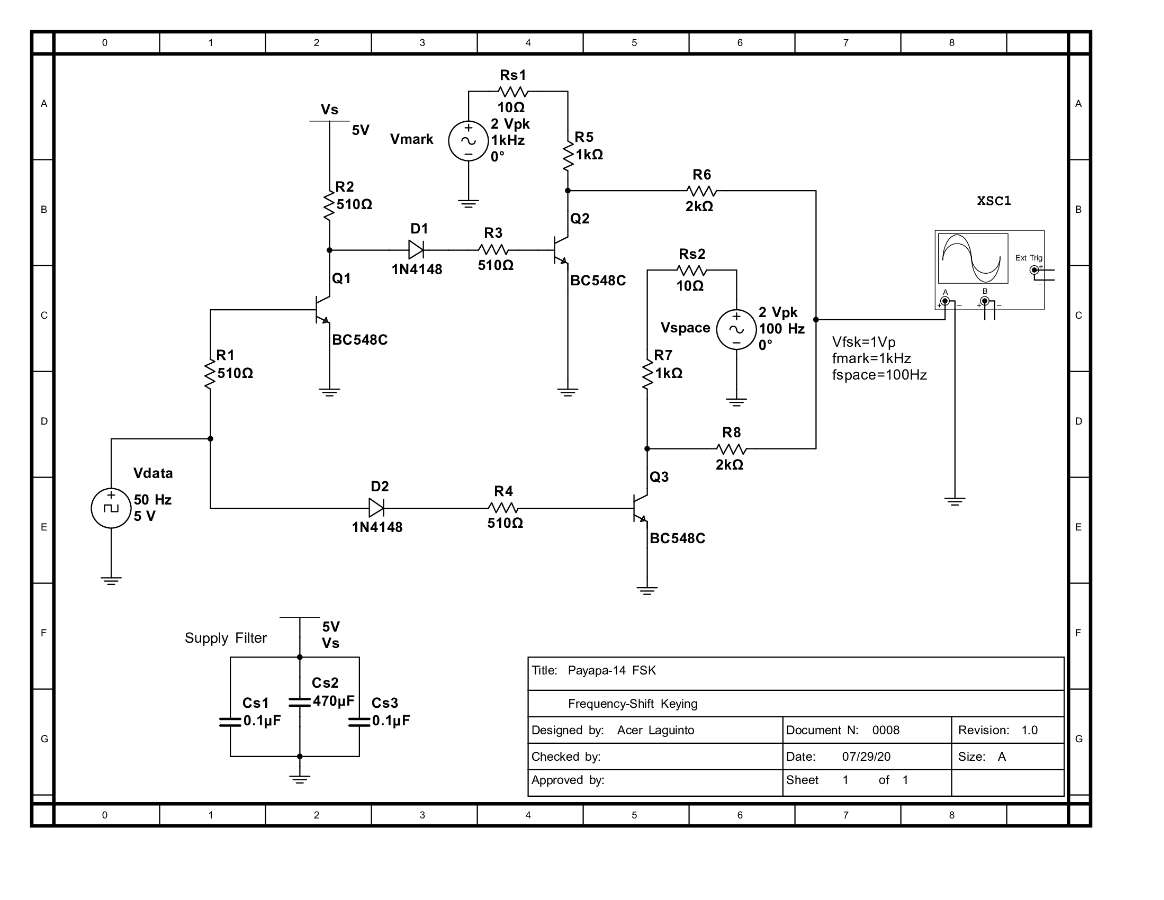
Components:
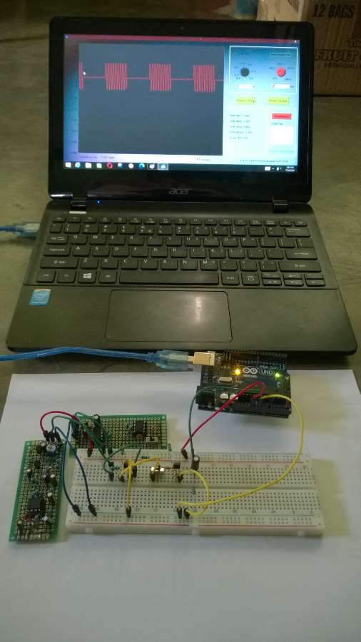
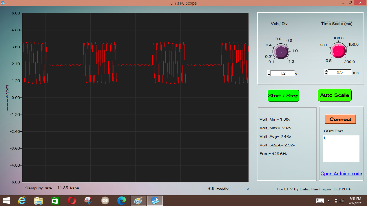
Again, connect the circuit in a breadboard to check the output waveform. Use the 100Hz sine wave oscillator as the space frequency, 1kHz sine as mark frequency, and the 50Hz/100Hz square as the data or modulating signal.
Screenshot of the FSK waveform in the EFY's scope:

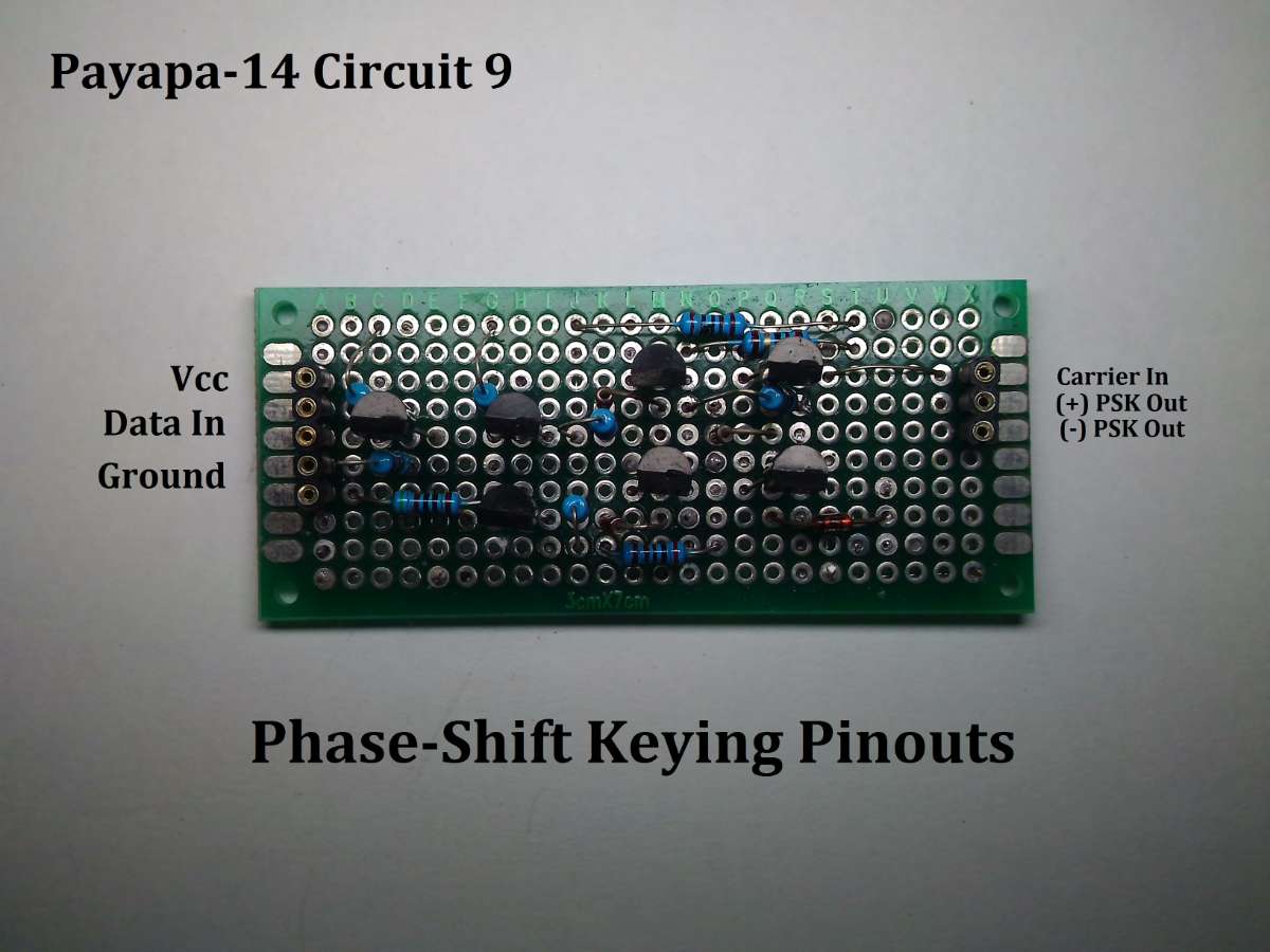
c. Phase-Shift Keying (PSK)
The Circuit:
If you will notice, the circuit for the PSK and the DSBSC are the same. This is because the action needed for PSK, which is the polarity inversion (180-degree phase shift), is also the action required for DSBSC. Consequently, unlike the previous and all the circuits, PSK/DSBSC output is not taken with respect to the ground but is taken across two non-ground points.
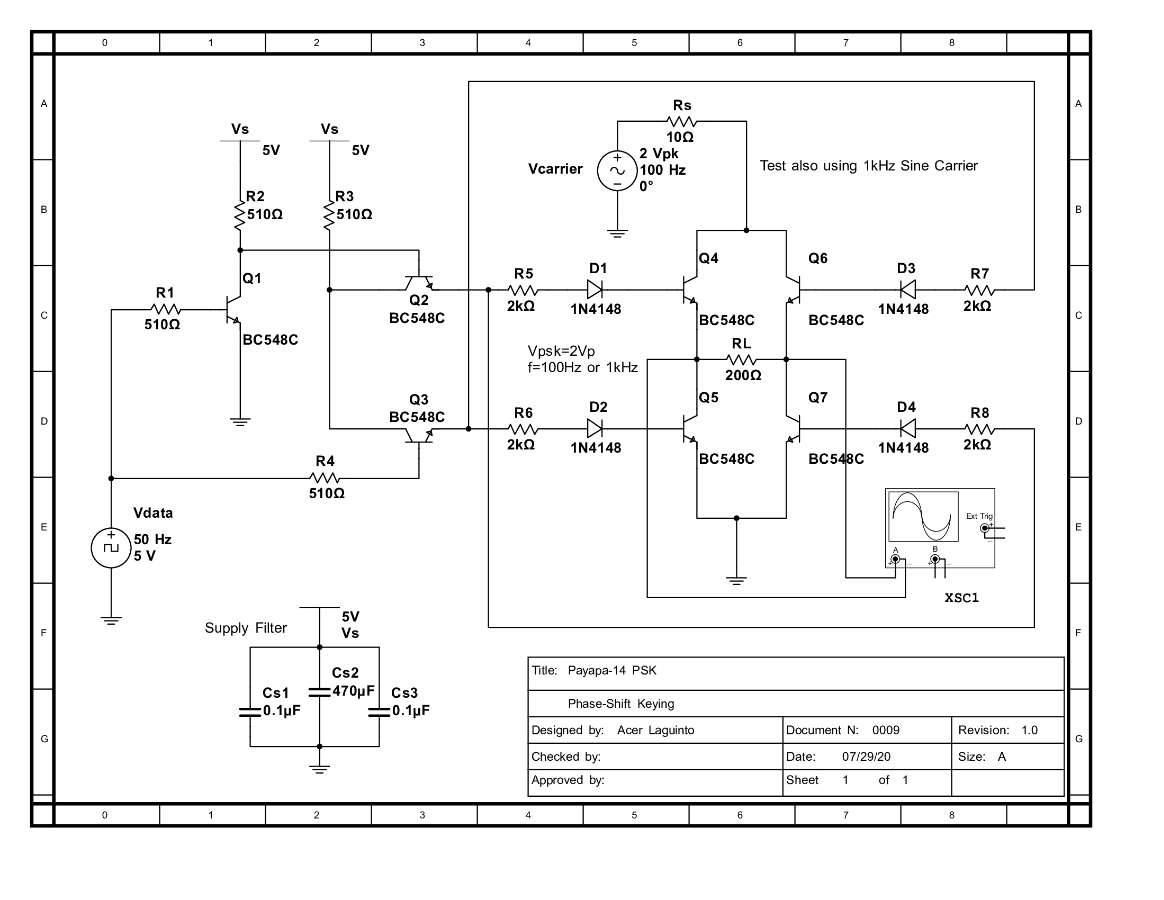
Components:
By wiring the components to the breadboard you should have:
For the input signals, use the 100Hz sine as the carrier, and 50Hz square as the data to get:
If the Carrier signal is changed to 1kHz, and the data to 100Hz the output should be:
Take note of the phase reversal in the output waveform.
Screenshot:
Circuit Building Part 4: Digital Transmission
a. Pulse Width Modulation (PWM)
b. Pulse Amplitude Modulation (PAM)
c. Pulse Position Modulation (PPM)
There are three basic and fundamental techniques in Digital Transmission: Pulse Width Modulation (PWM), Pulse Amplitude Modulation (PAM), and Pulse Position Modulation (PPM).
For the entire Digital Transmission Circuits, the modulating signal or the input signal is the 100Hz sine wave.
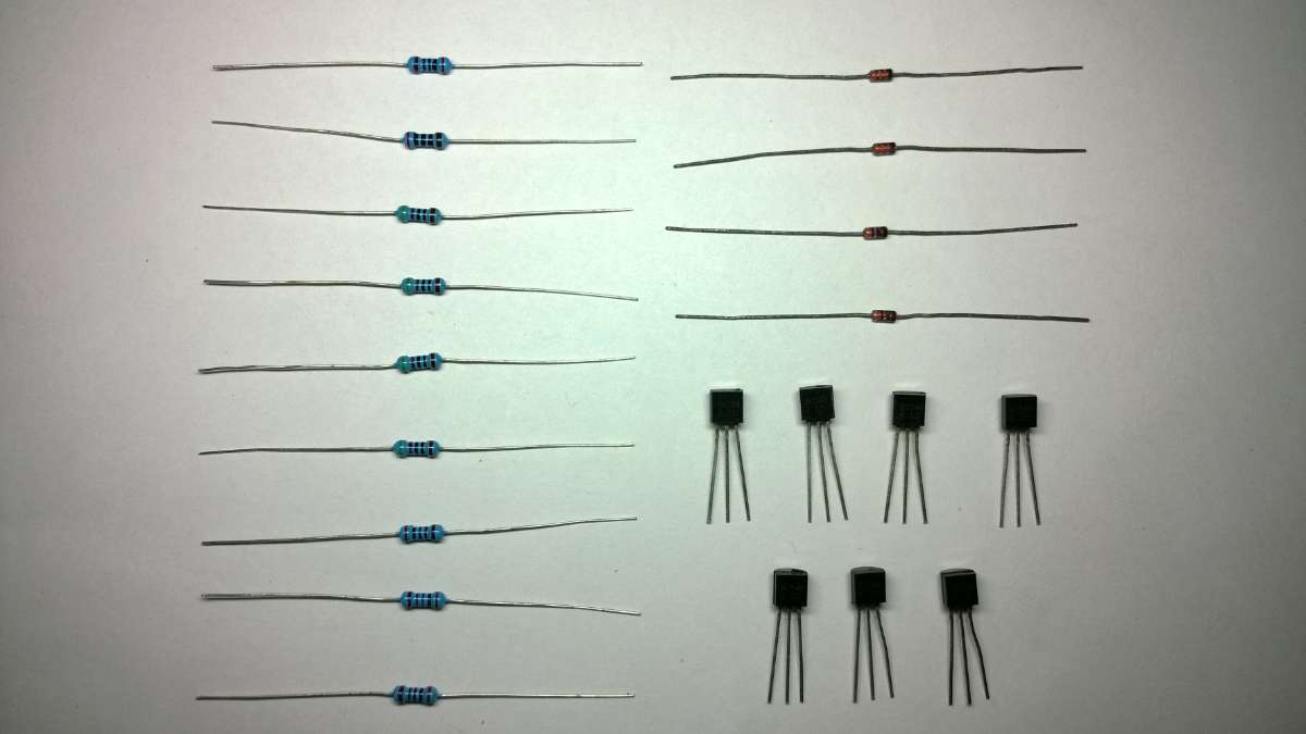
a. Pulse Width Modulation (PWM)
The Circuit:
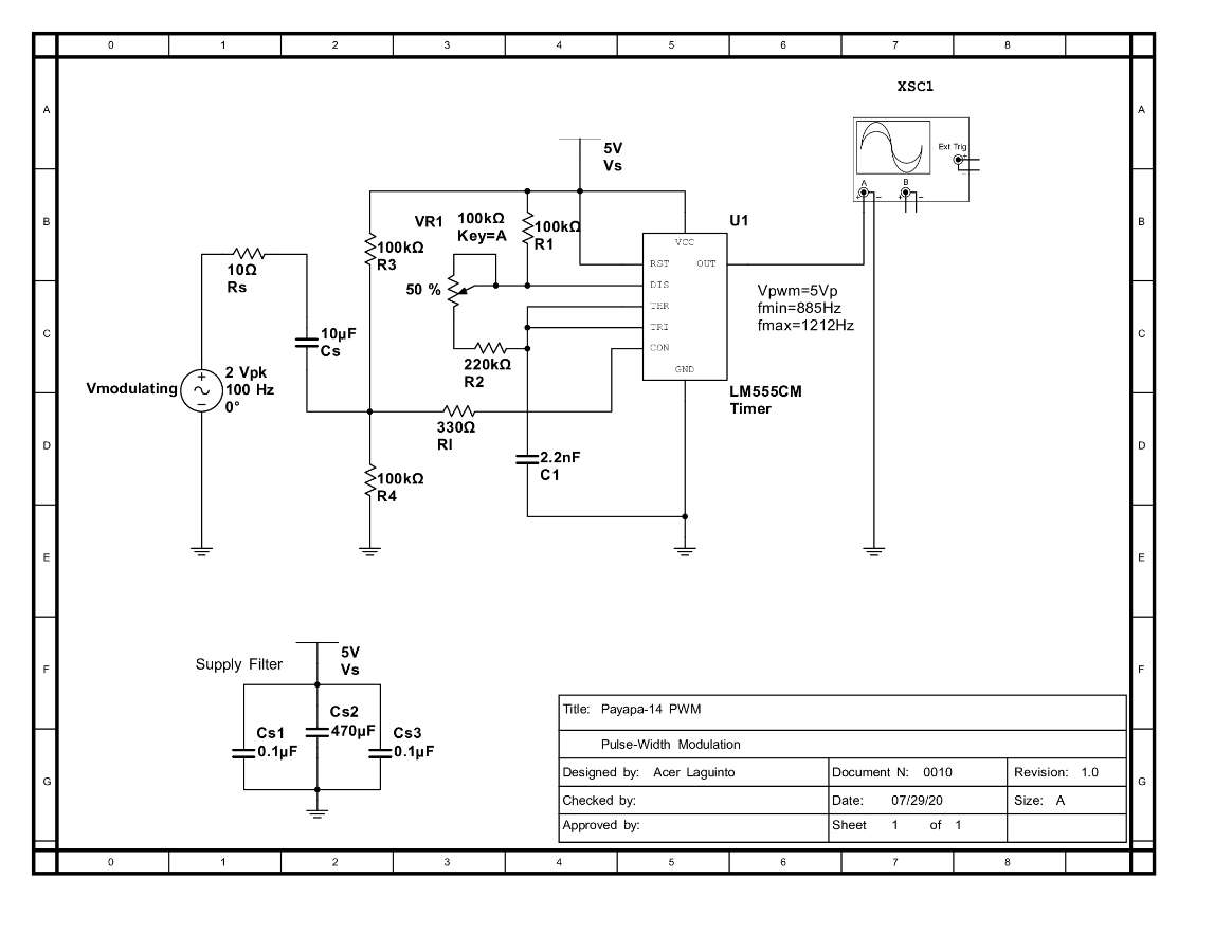
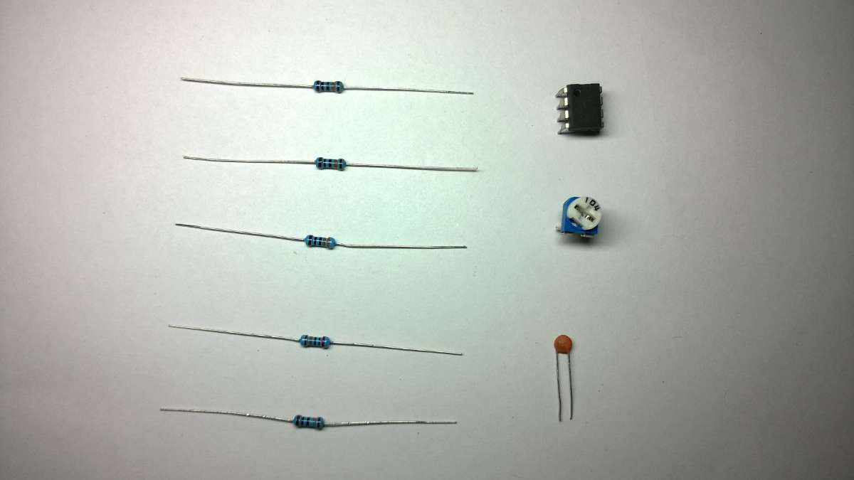
Components:
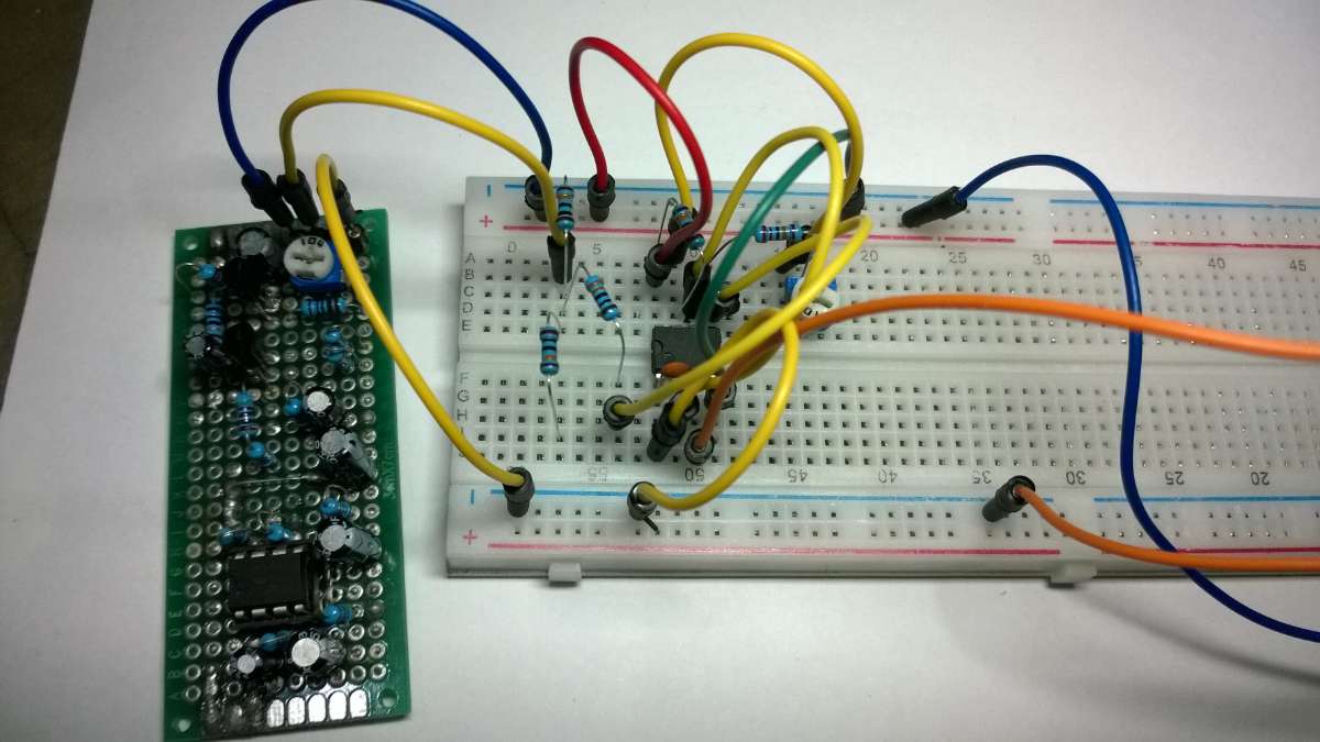
Breadboard test, the connection should be like:
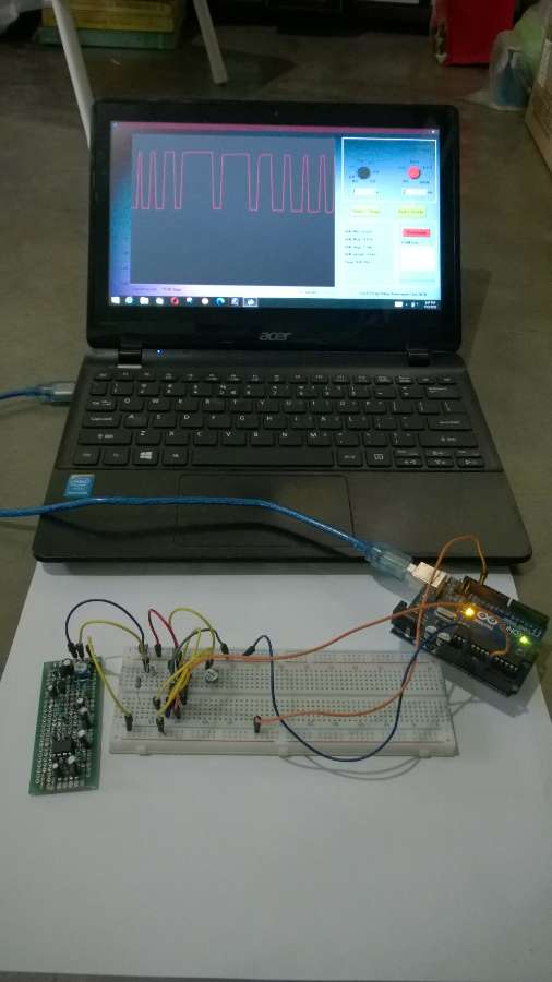
Use the 100Hz Sine wave oscillator as the modulating signal. So that the output waveform looks like:
You can vary the carrier pulse frequency via the trimmer:
Screenshot:
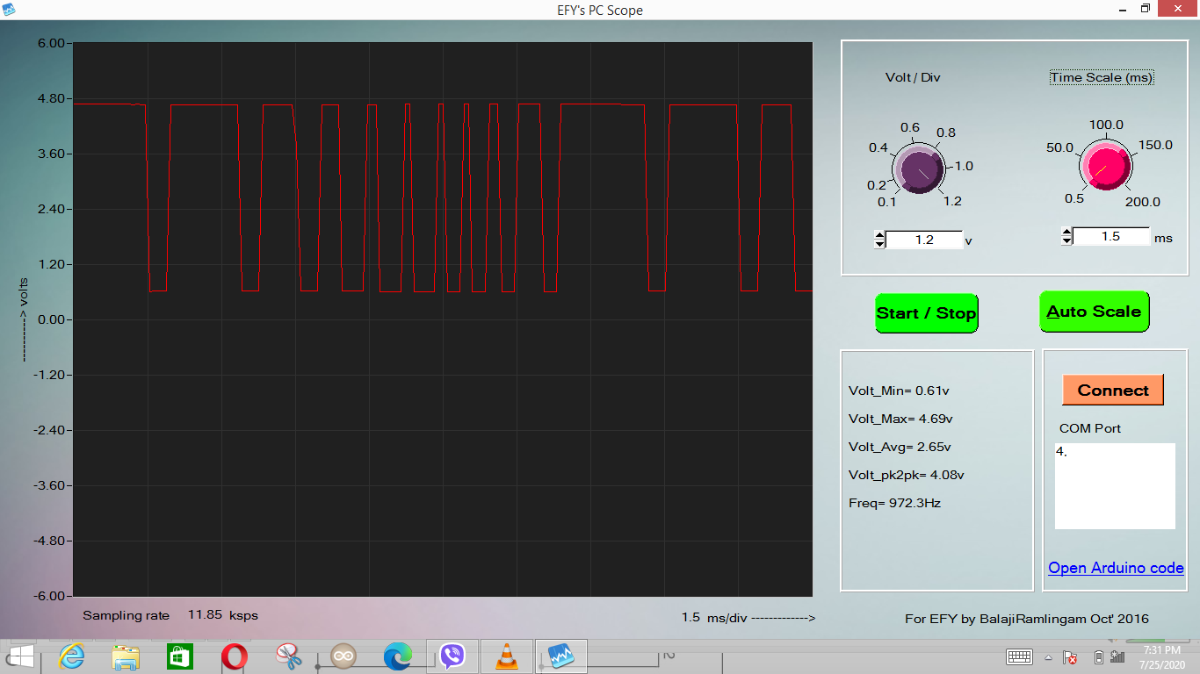
b. Pulse Amplitude Modulation (PAM)
There are two types of PAM; the Natural PAM and the Flat-top PAM.
i. Natural PAM
The Circuit:
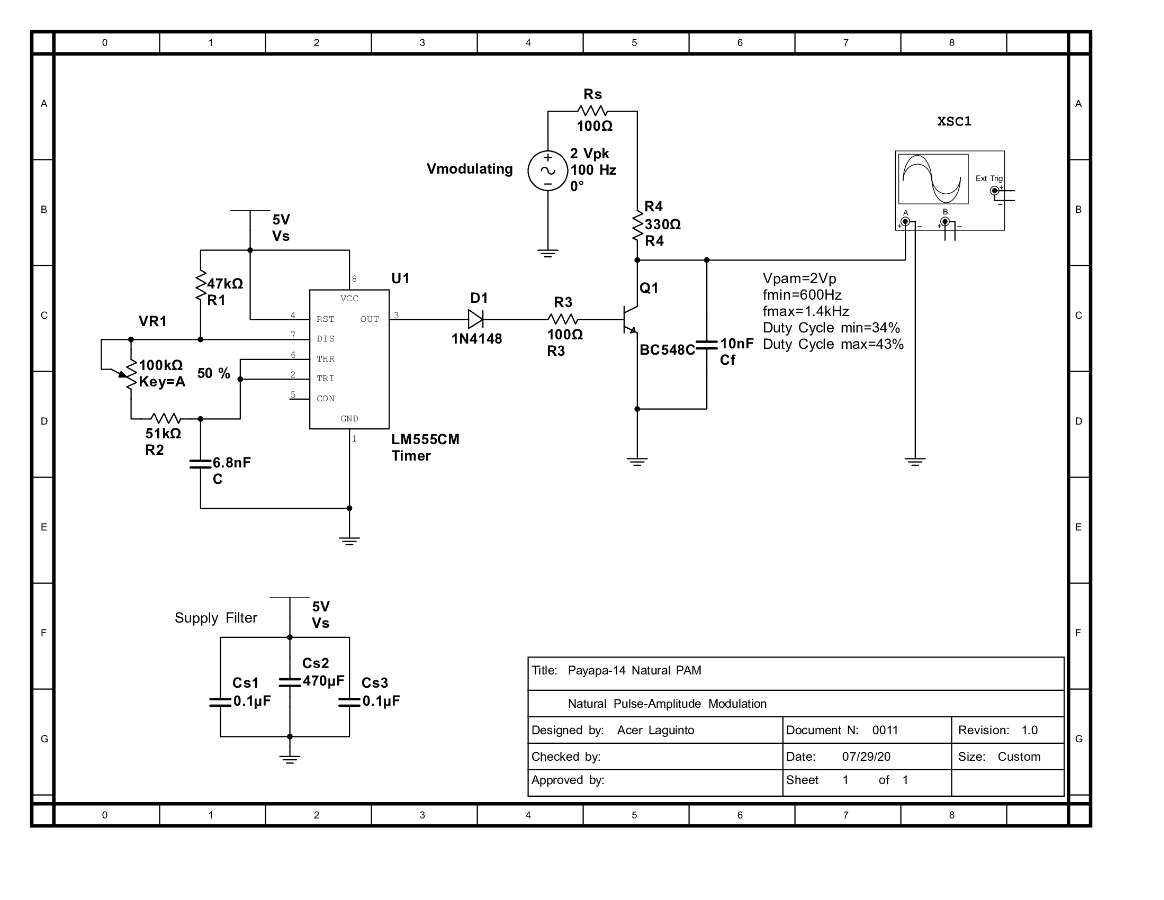
Components:
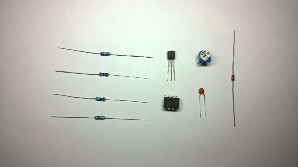
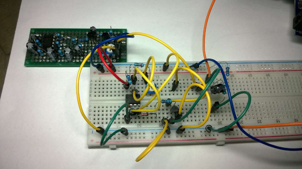
In breadboard, connect the components by following the schematic:
The output waveform should be:
Screenshot:
ii. Flat-Top PAM
The Circuit:
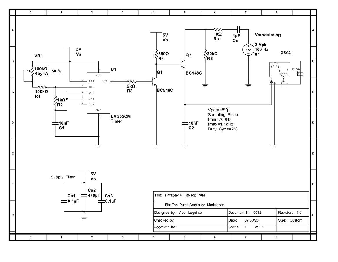
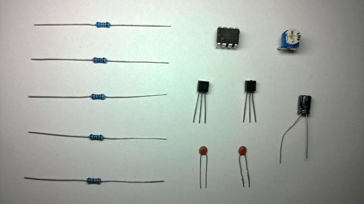
Components:
Verify the output using breadboard before soldering on the pcb:
In which you should get:
Screenshot:
.png)
c. Pulse Position Modulation
The Circuit:
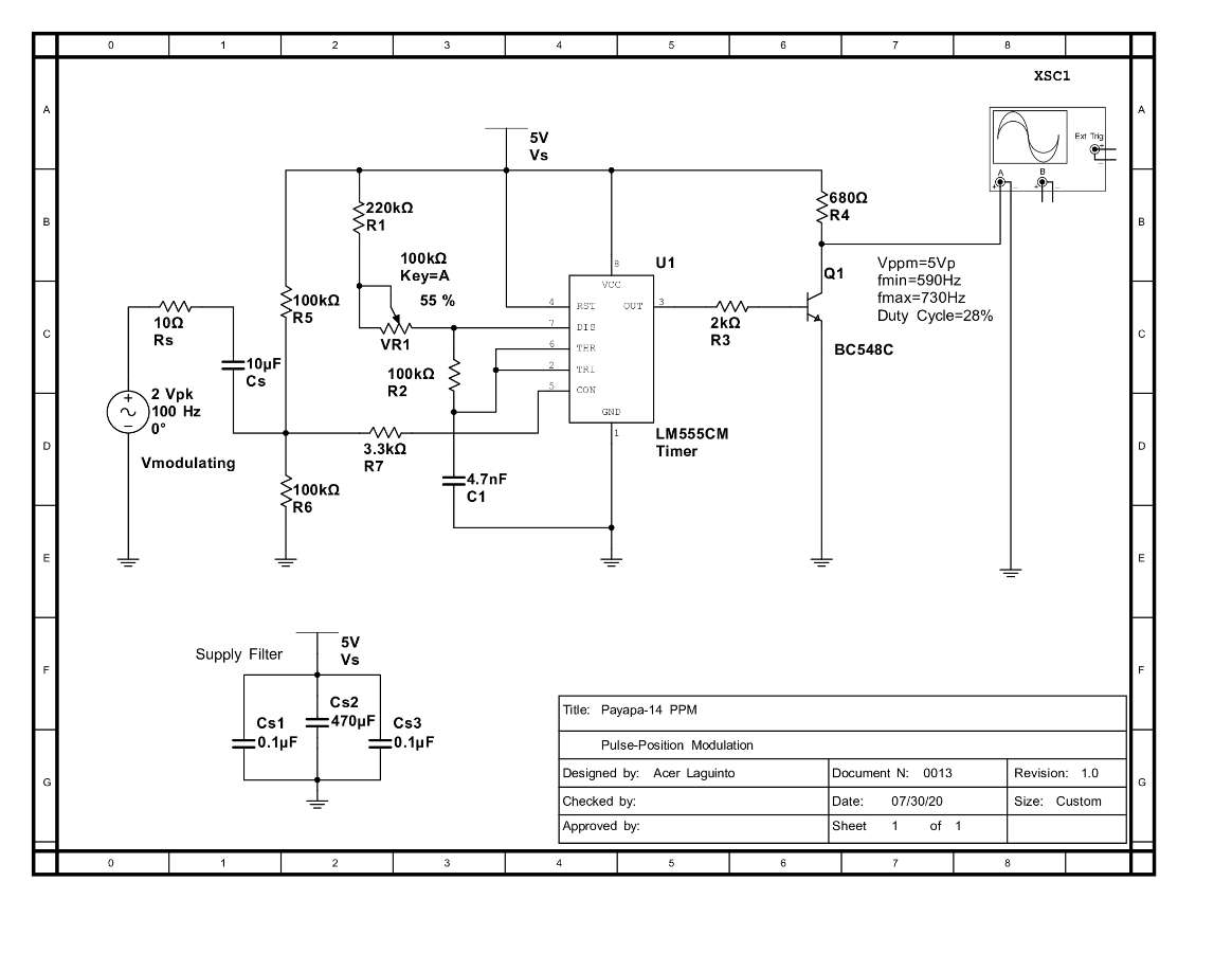
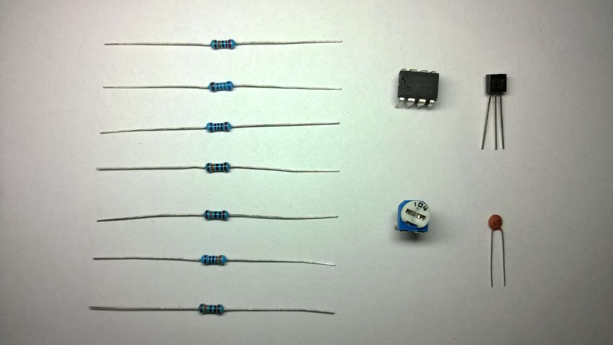
Components:
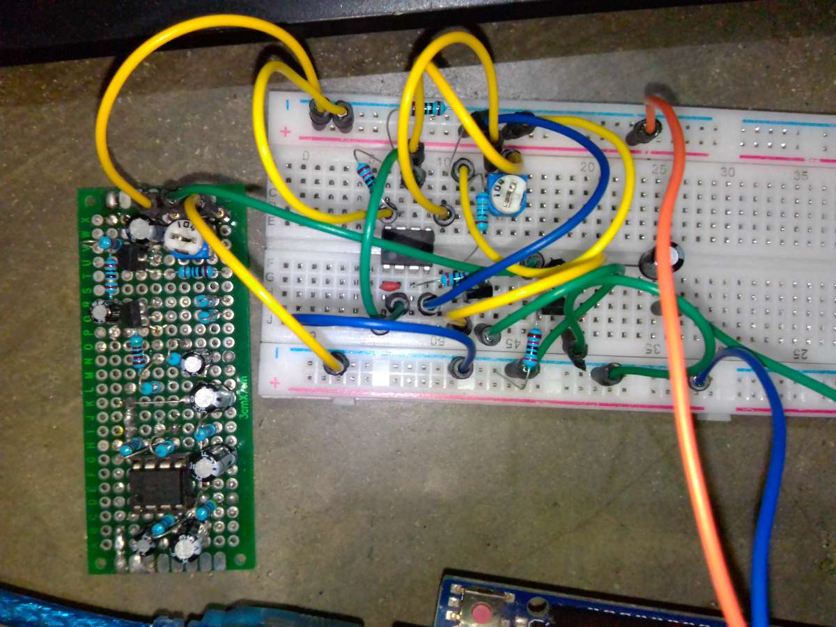
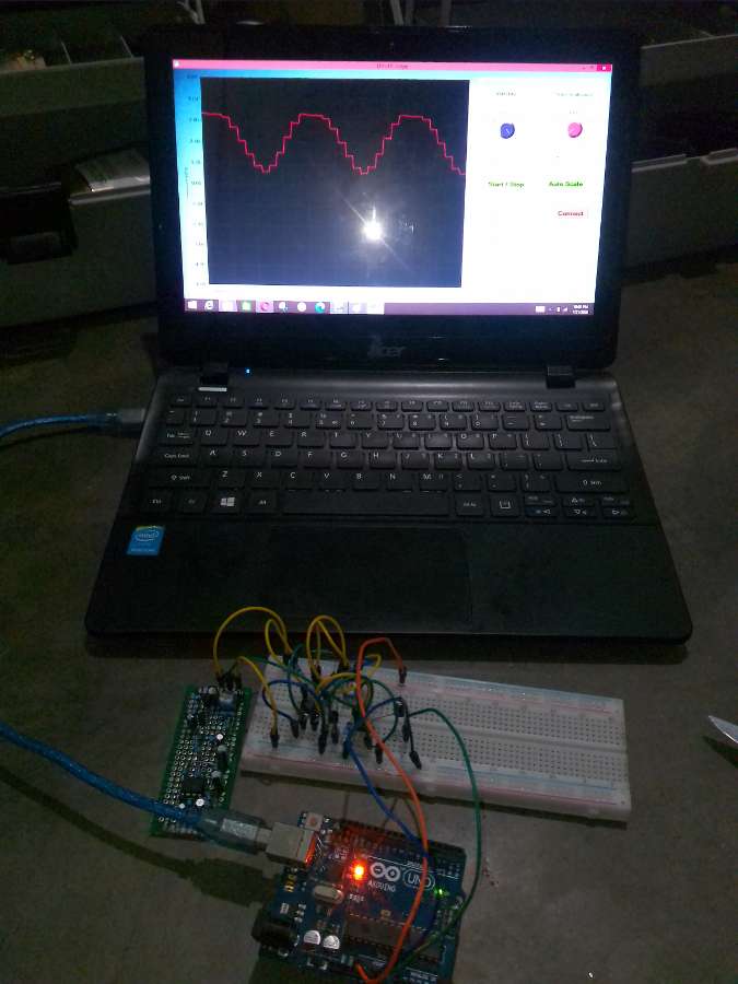
Again, check the output signal first using a breadboard:
The output Waveform should be:
Screenshot:
C. OUTPUT
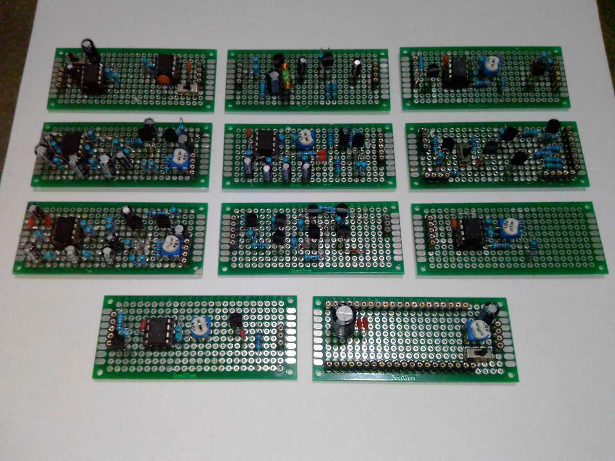
Once the output waveform is correct, you can proceed soldering the components on the PCB. In this project, universal PCB was used in order to save time in the layout and etching.
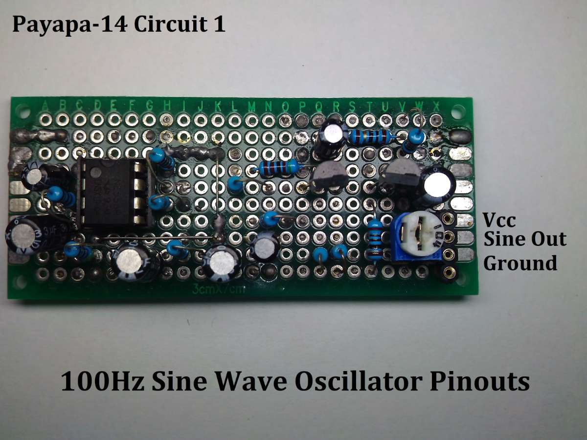
1. 100Hz sine Wave Oscillator
.jpg)
The Pinouts:
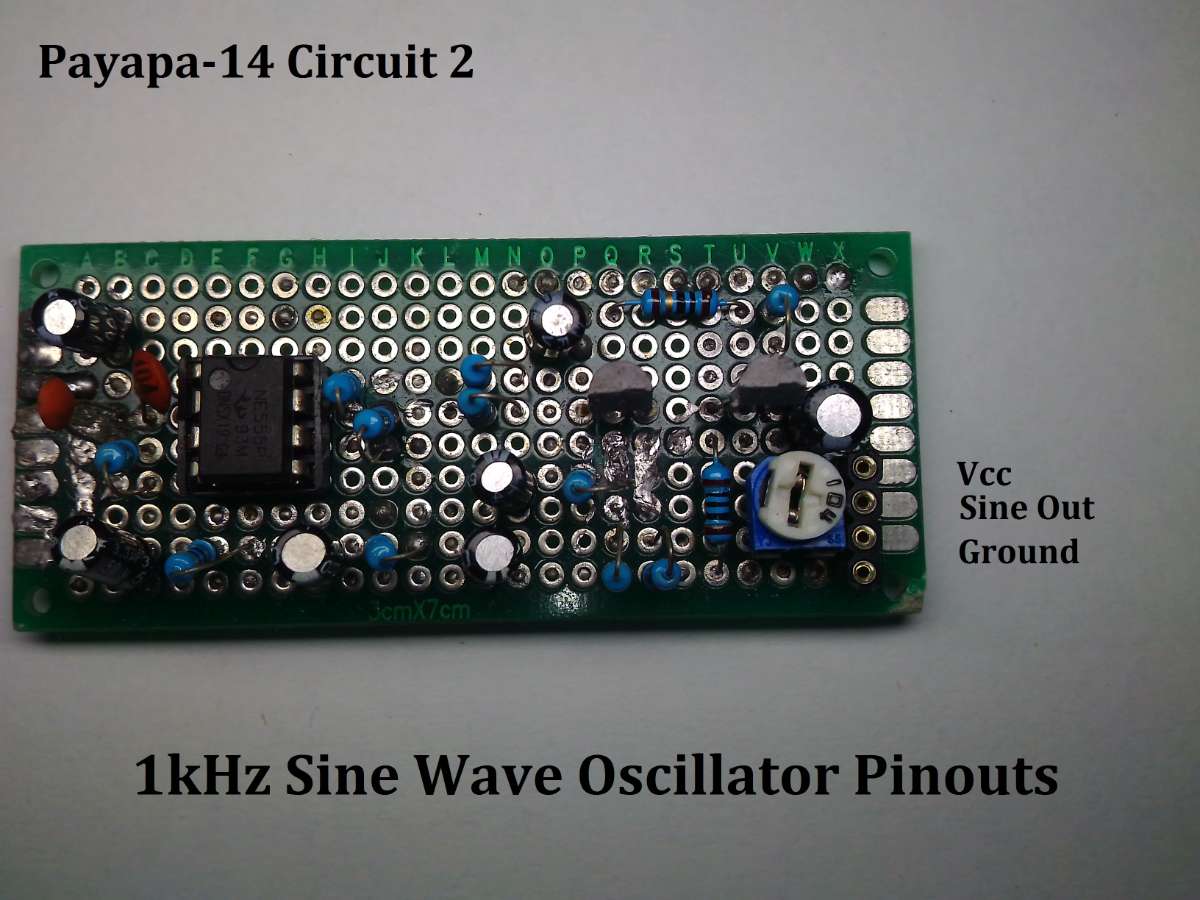
2. 1kHz Sine Wave Oscillator
.jpg)
The Pinouts:
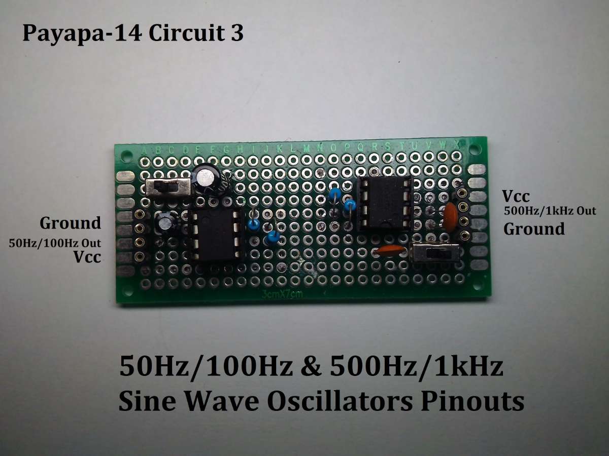
3. 50Hz/100Hz & 500Hz/1kHz Square Wave Oscillator
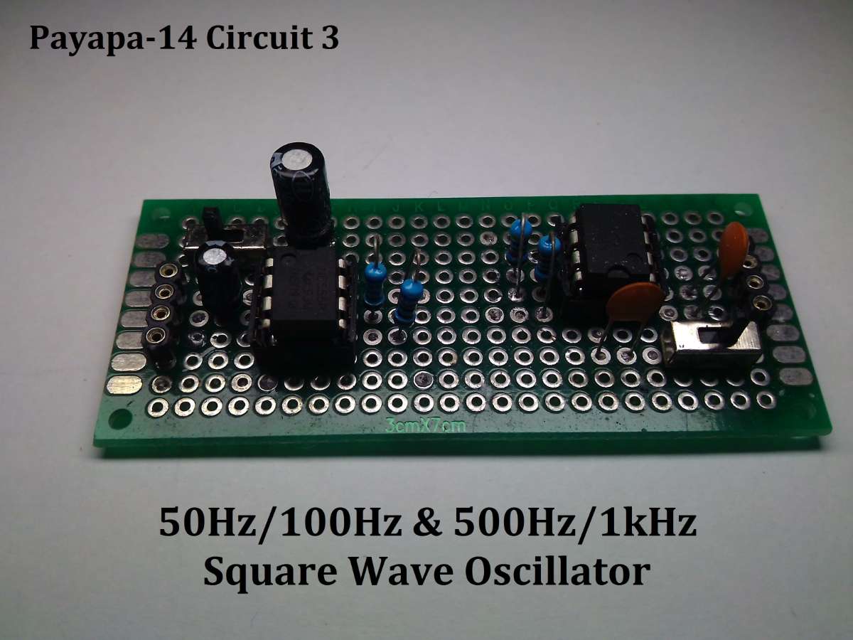
The Pinouts:
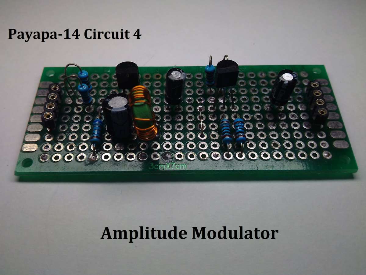
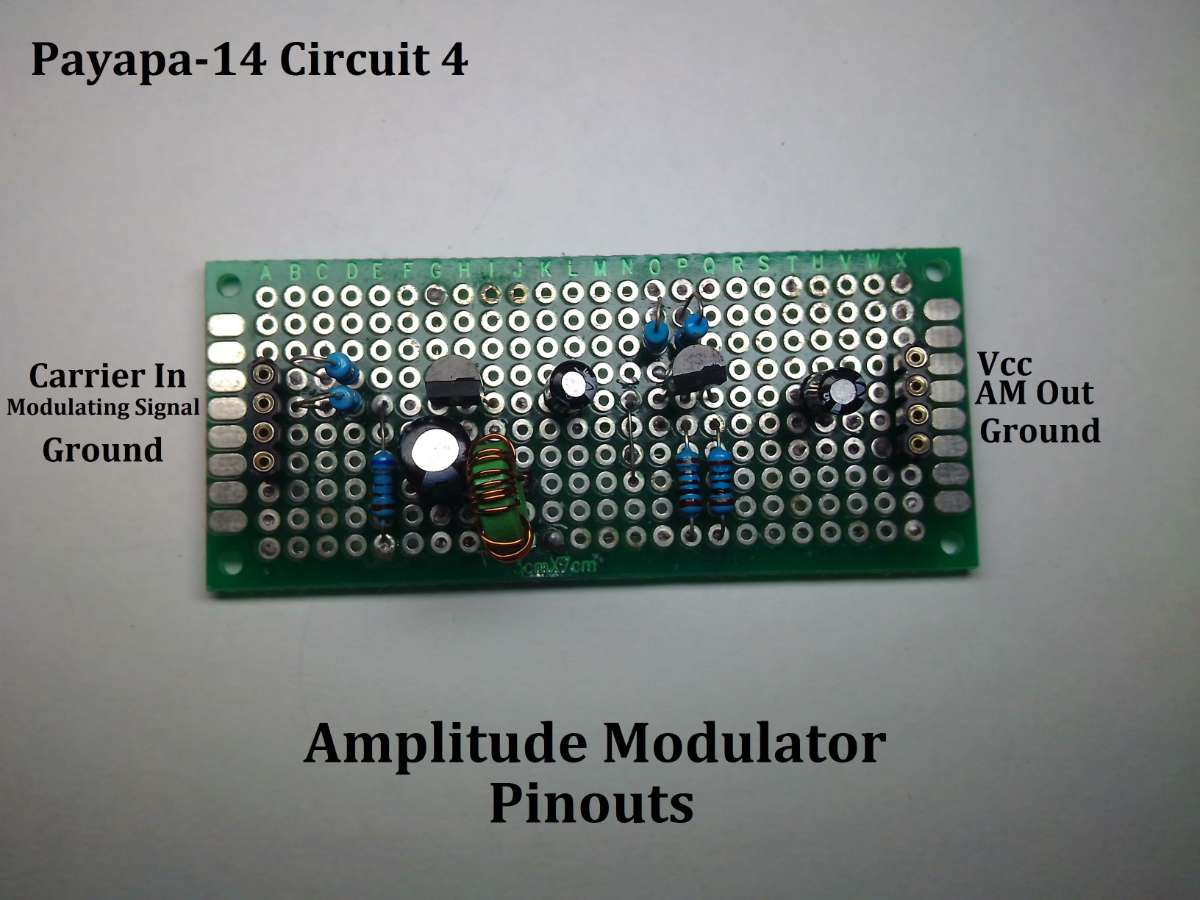
4. Amplitude Modulator
The Pinouts:
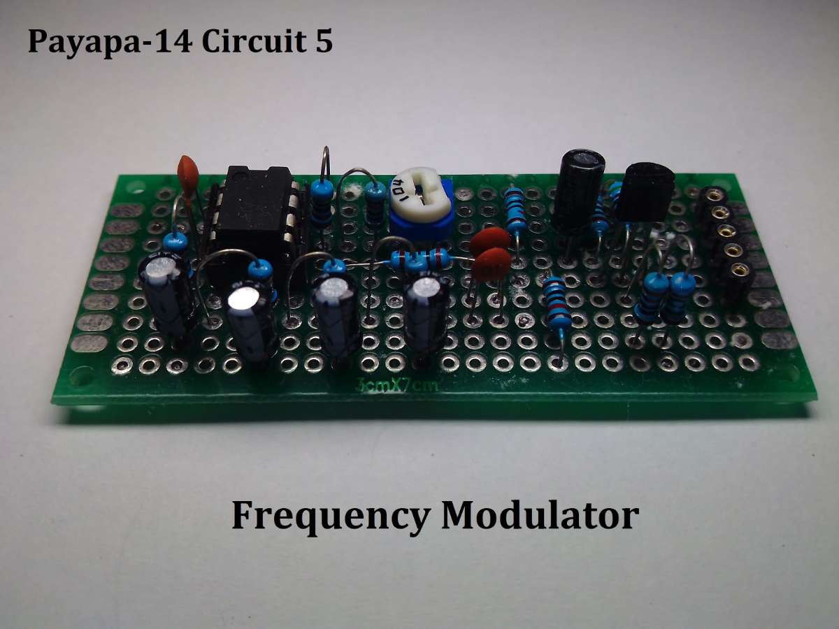
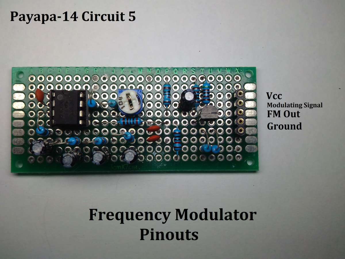
5. Frequency Modulator
The Pinouts:
6. Double-Sideband Suppressed Carrier AM
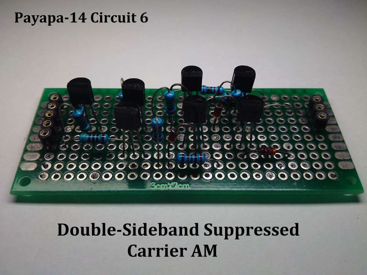
The Pinouts:
7. Amplitude-Shift Keying & Frequency-Shift Keying
The Pinouts:
8. Phase-Shift Keying
.jpg)
The Pinouts:
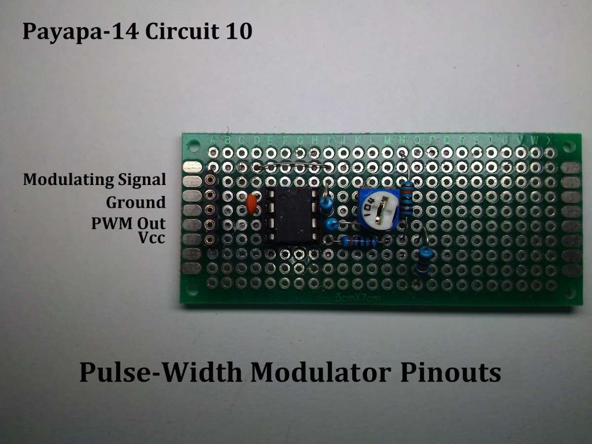
9. Pulse-Width Modulator
.jpg)
The Pinouts:
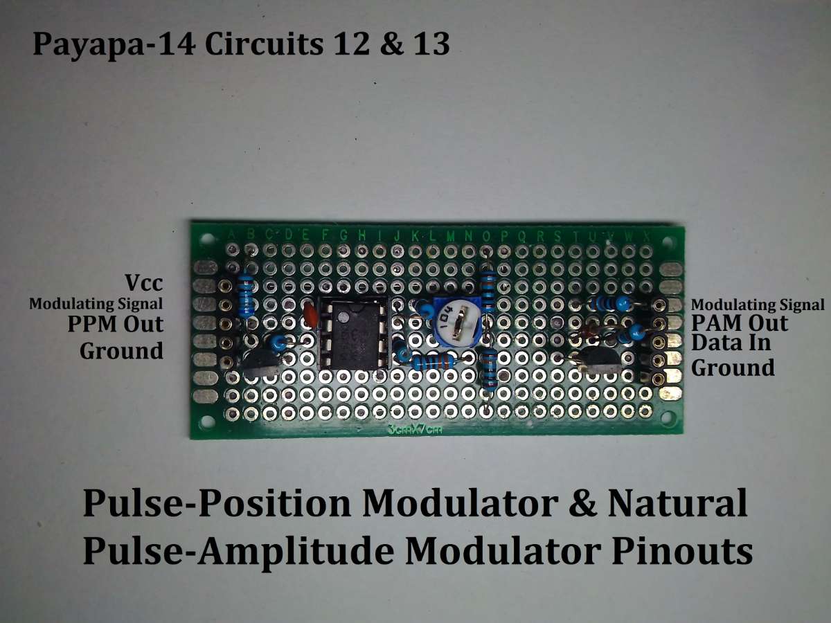
10. Pulse-Position Modulator & Natural Pulse-Amplitude Modulator
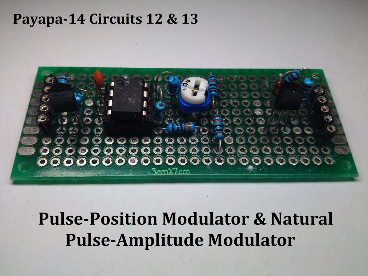
The Pinouts:
11. Flat-Top Pulse-Amplitude Modulator
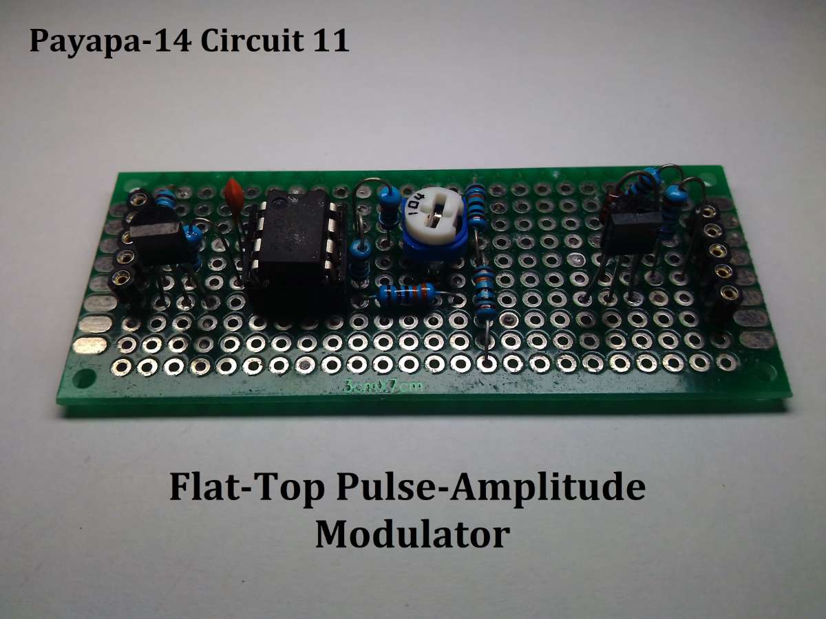
The Pinouts:
.jpg)
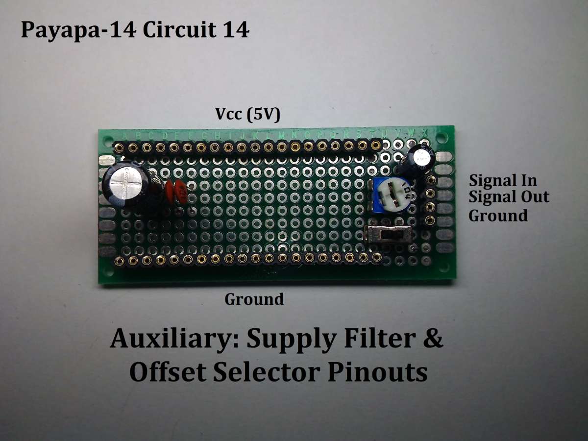
12. Auxiliaries
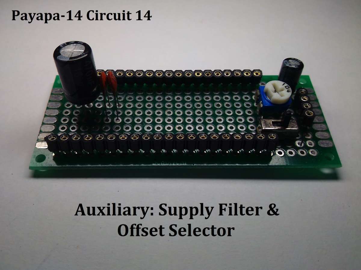
The Pinouts:
Final Video: