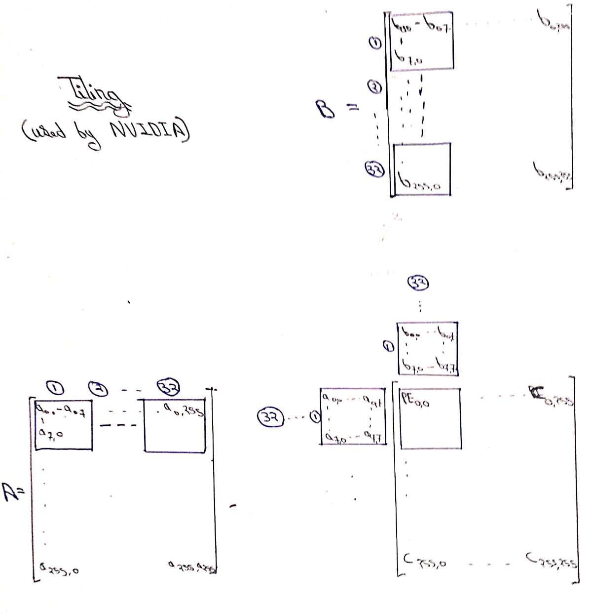
Tiled Systolic Array for Matrix Multiplication on an FPGA

Phase 1: Architectural Design & Mathematics
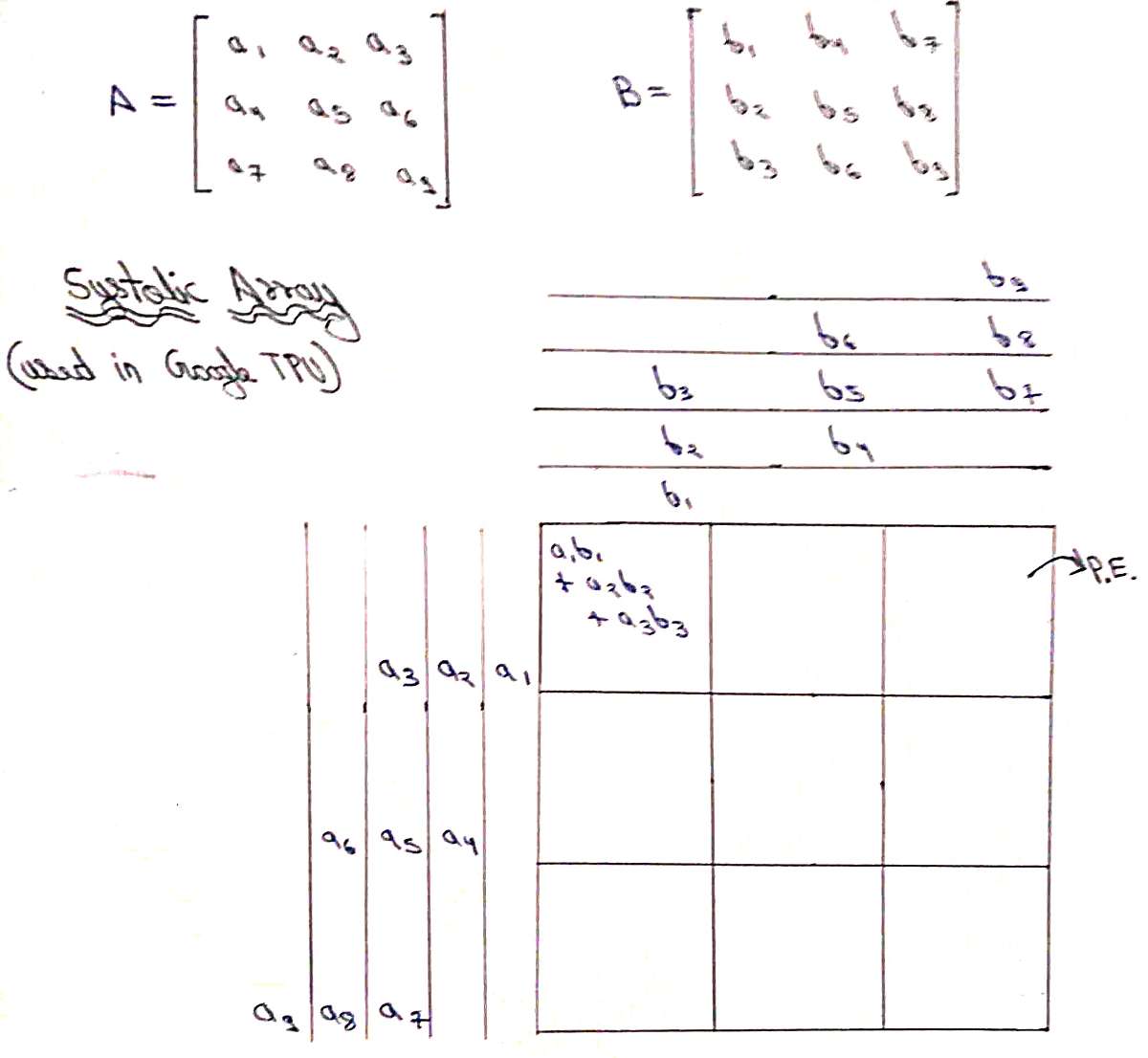
- Understand the Math and Dataflow: * Break down a large matrix multiplication (e.g., 256 times 256) into smaller blocks called "tiles" (e.g., 8 times 8 sub-blocks).
- Choose your number representation. For standard deep learning or signal processing hardware accelerators, use signed numbers.
- Define the Hardware Scale: * Decide on your physical hardware boundaries. In this architecture, i build an 8 times 8 mesh of Processing Elements (PEs).
Design the Core Element (The PE): * Sketch out a single Processing Element (PE). It should feature a Multiply-Accumulate (MAC) unit along with local data-forwarding registers.
Phase 2: Hardware Description (HDL) Development
- Code the Processing Element (PE): * Write the Verilog or SystemVerilog code for a single PE. Map the MAC unit to utilize the FPGA's built-in DSP48 slices specifically configured for 8-bit signed multiplication and 32-bit signed accumulation.
- Build the Systolic Mesh: * Instantiate an $8 \times 8$ grid of your written PEs. Wire them structurally so that each PE only communicates with its immediate neighboring PEs (no global wiring bus for data movement).
Implement the Control Logic (FSM): * Write a Finite State Machine (FSM) to handle the 3 execution phases: loading data from memory, running the MAC operations, and shifting out the finalized matrix results.
- Ensure your FSM rhythmically "pulses" data through the grid side-by-side using valid-bit propagation.
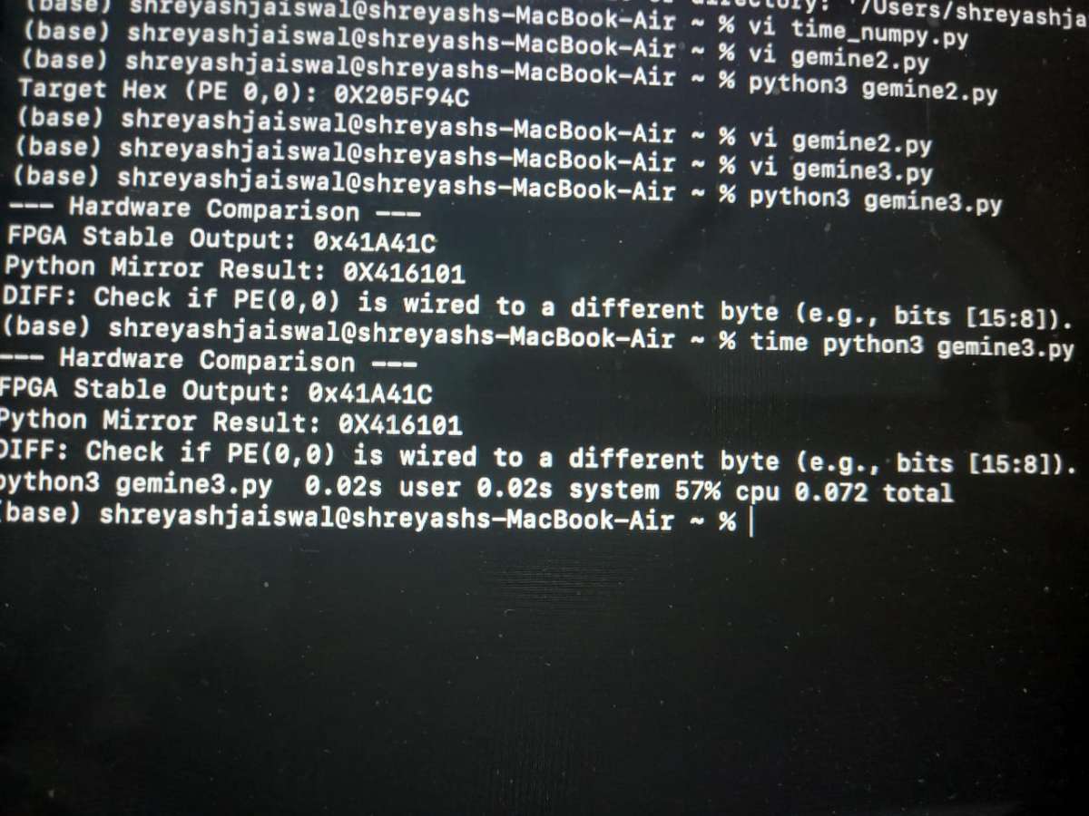
Phase 3: Software Verification (The Golden Model)
- Create a Bit-True Software Model: * Write a Python script that perfectly mimics how your hardware computes matrix math at a bit-level (using 8-bit signed inputs and 32-bit accumulation limits).
Generate Test Vectors: * Use this Python "Golden Model" to generate random matrices, calculate the expected outputs, and export them as test data files.
Phase 4: Simulation & Testing
- Write a Testbench: * Create an HDL testbench that reads your Python-generated test files, streams the inputs into your 8 times 8 grid, and captures the outputs.
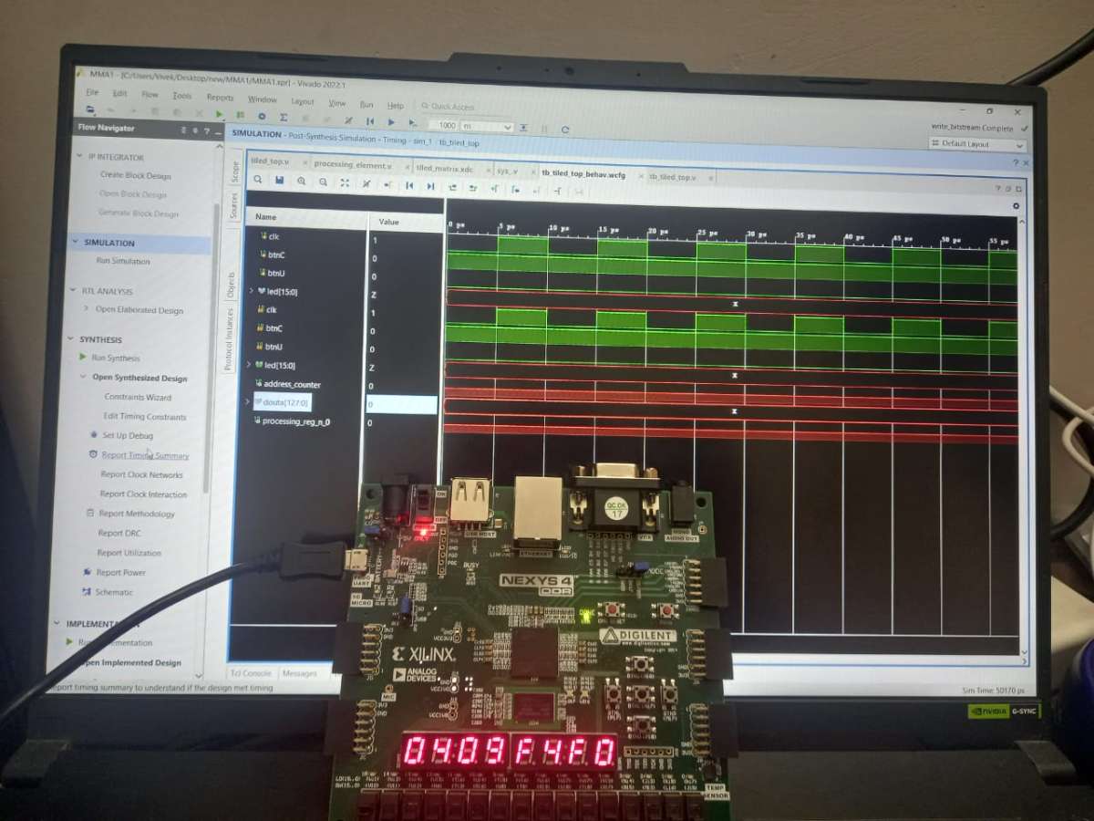
- Verify Cycle Counts & Performance: * Run a cycle-accurate simulation (using tools like Vivado Simulator or ModelSim).
- Verify that a full matrix pass takes exactly 256 + 15 clock cycles, where 256 cycles are for streaming data and 15 cycles (+15 pipeline latency) are for filling and draining the 8 times 8 systolic pipeline.
Compare Hardware Outputs: * Check that your simulated hardware outputs perfectly match your software's golden reference targets.
Phase 5: FPGA Synthesis and Deployment
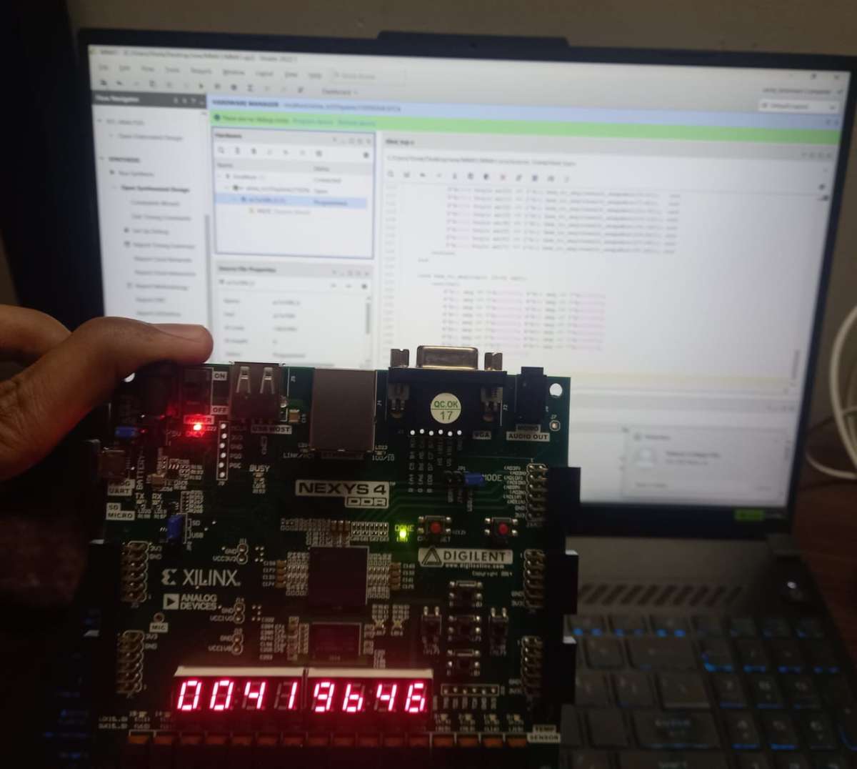
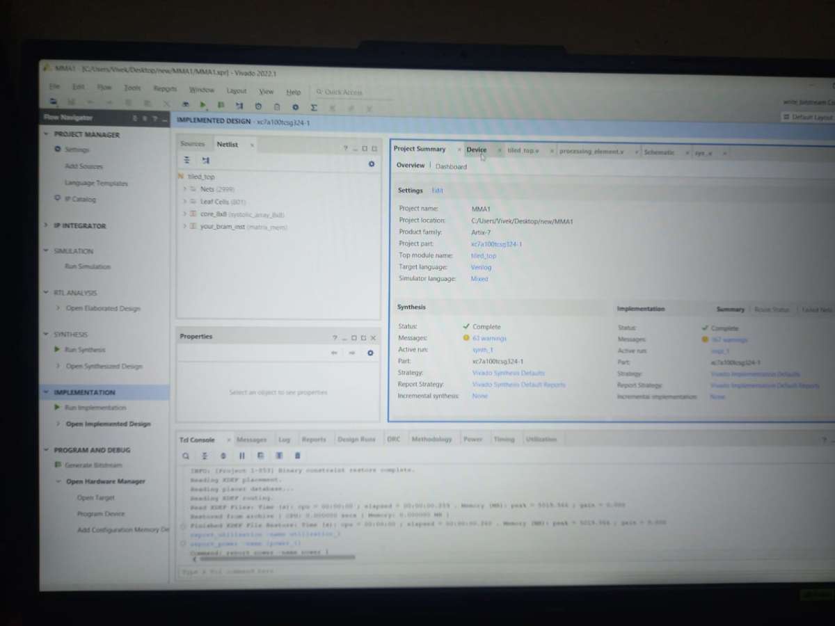
- Synthesize & Constrain: * Import your design into an FPGA toolchain (like AMD Xilinx Vivado). Define your clock frequency constraints.
- Run Synthesis and Implementation to map your structural grid design explicitly onto physical FPGA lookup tables (LUTs), flip-flops, and DSP48 blocks.
Generate Bitstream & Run: * Generate the final programming bitstream file and load it onto your physical FPGA development board to accelerate your tiled matrix operations in hardware!.
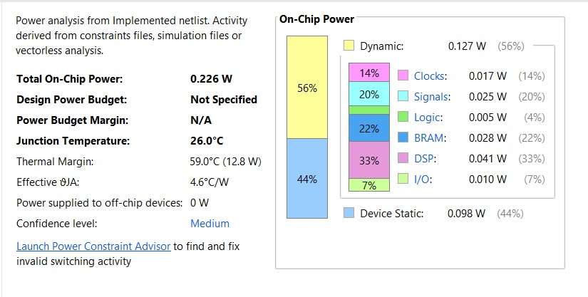
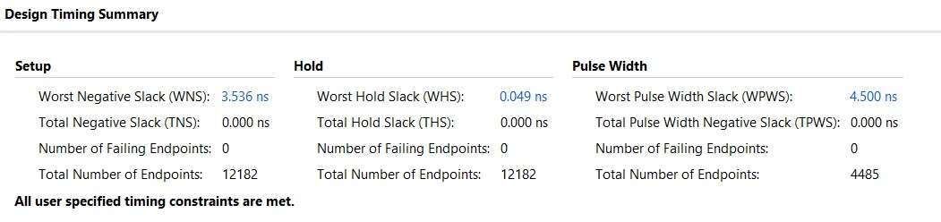
Check reports
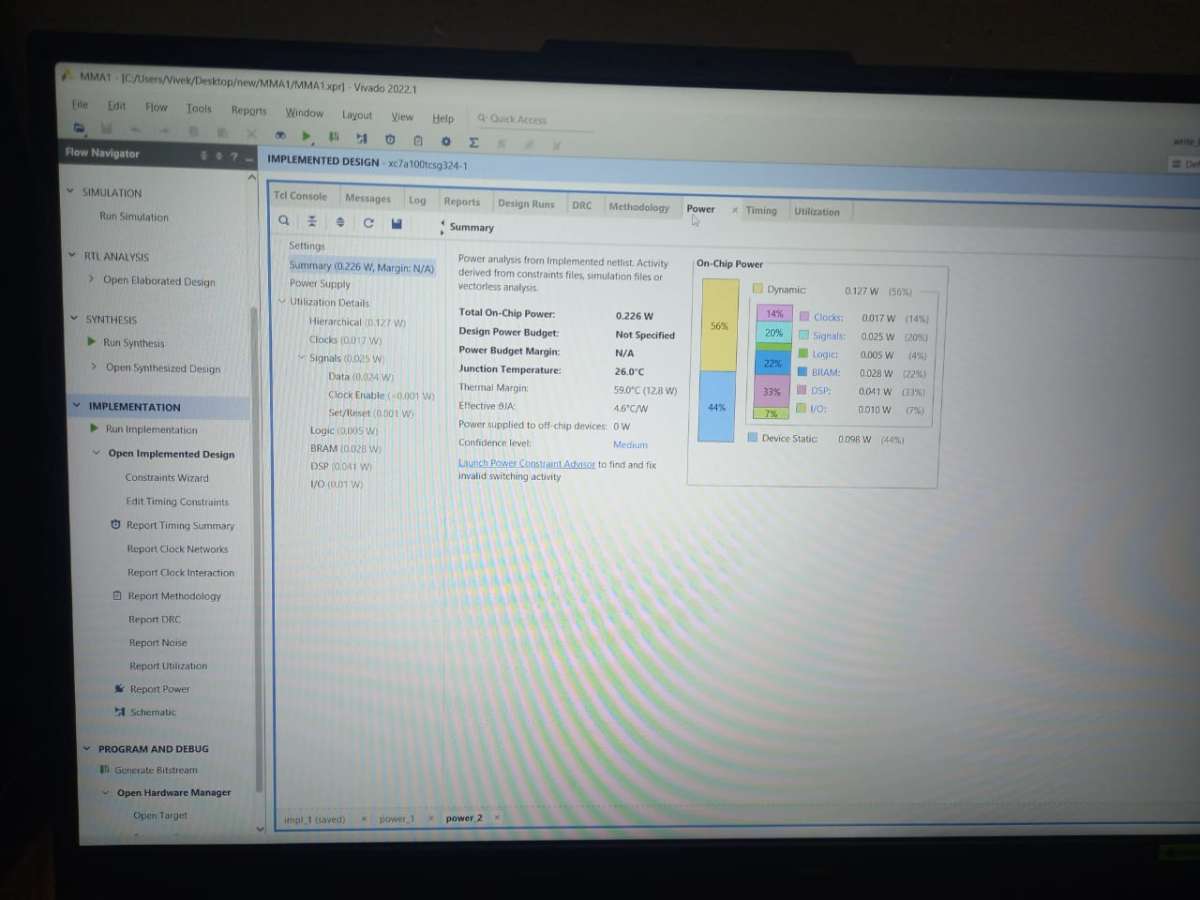
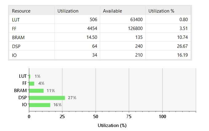
Check Hardware utilization
youtube link: